A structure-optimized white light organic EL part

An electroluminescent device, an organic technology, applied in the direction of electric solid-state devices, electrical components, semiconductor devices, etc., can solve the problems of a wide variety of organic materials, complicated preparation processes, etc., reduce the preparation cost and production process, simplify the preparation process, good stability effect

Inactive Publication Date: 2008-02-13
UNIV OF ELECTRONIC SCI & TECH OF CHINA
View PDF4 Cites 12 Cited by
  • Summary
  • Abstract
  • Description
  • Claims
  • Application Information

AI Technical Summary

Problems solved by technology

[0006] The technical problem to be solved by the present invention is how to provide a structure-optimized white light organic electroluminescence device and its preparation method. White light emission reduces the cost of raw materials and is more suitable for industrial produc

Method used


Image

  • A structure-optimized white light organic EL part
  • A structure-optimized white light organic EL part

Examples


Embodiment 1

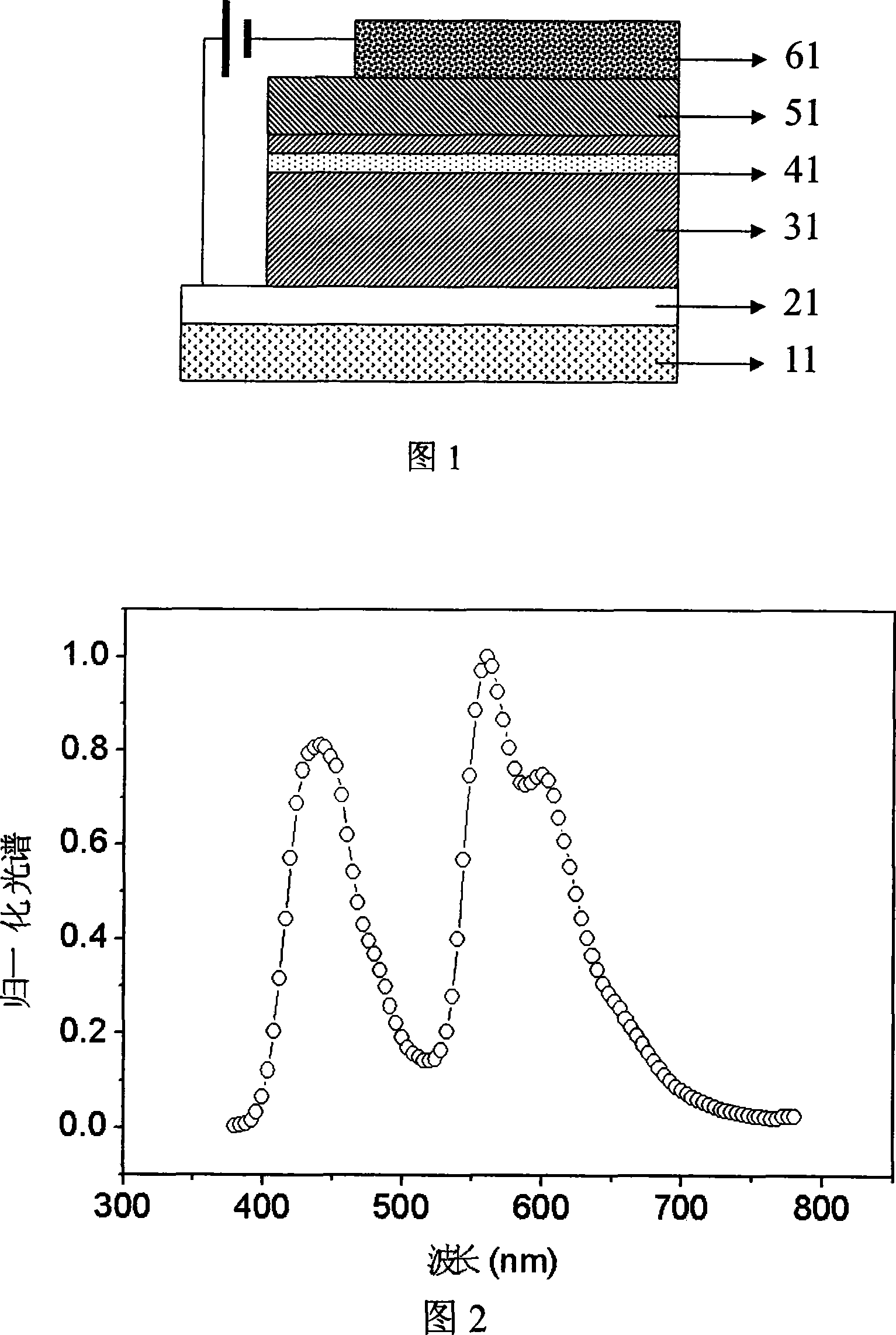
[0047] The device structure of this embodiment is shown in FIG. 1 , the device substrate 11 is glass, and the anode layer 21 used is an indium tin oxide (ITO) film. Obtain the required anode layer 21 pattern on the ITO film by photolithography, then ultrasonically clean it with lye, acetone, ethanol, and deionized water, and dry it with high-purity nitrogen before use; put the cleaned ITO substrate into the pretreatment chamber body, in a vacuum higher than 10 -6 After Torr, an appropriate amount of nitrogen and oxygen is introduced for plasma treatment to improve the work function of the ITO film. After the pretreatment is completed, it is directly transferred to the organic thin film evaporation chamber; in a high vacuum environment, start to evaporate the hole transport layer 31NPB with a thickness of 40nm; then close the baffle of the substrate and open the doping material (t-bt) 2 The evaporation power supply of Ir (acac), after reaching the required rate, open the baffl...

Embodiment 2

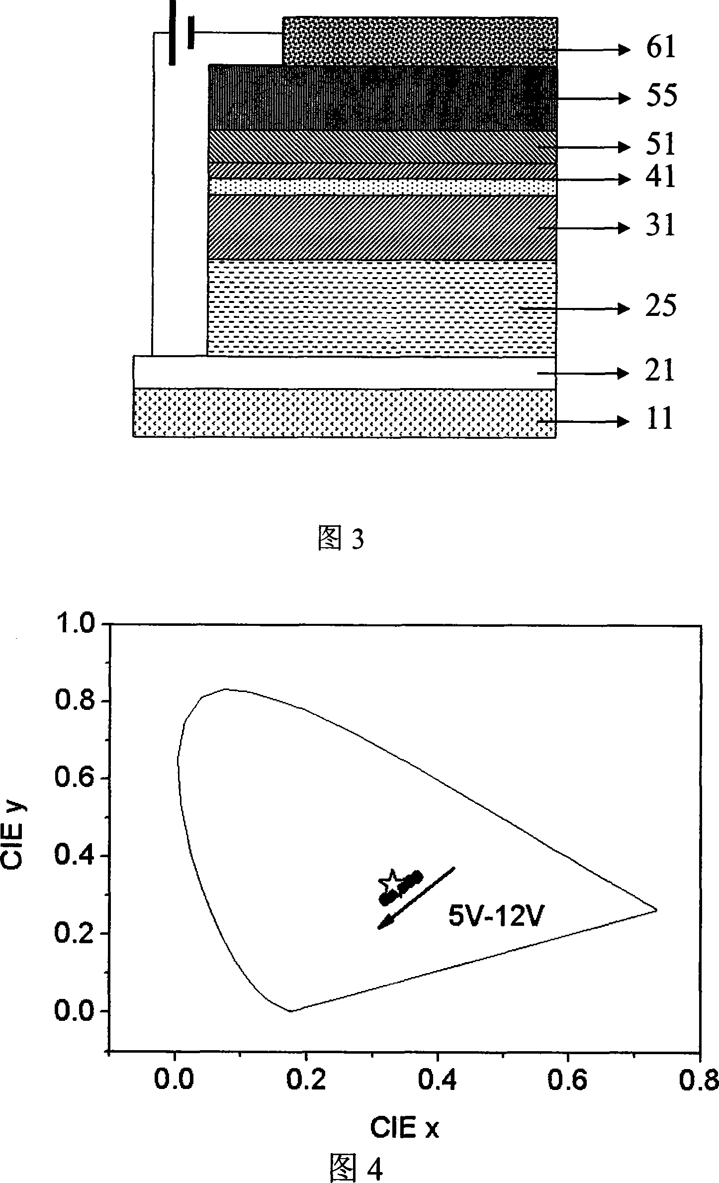
[0050] On the basis of Example 1, we increase the hole injection layer 25 between the anode layer 21 and the hole transport layer 31, and the yellow light doping material (t-bt) 2 Ir(acac) is replaced by Rubrene, and an electron injection layer 55 is added between the hole blocking layer 51 and the cathode 61 . The device structure is shown in Figure 3, and the materials and layer thicknesses used are: ITO / CuPc (30nm) / NPB (30nm) / NPB: Rubrene (0.4%, 30nm) / NPB (1nm) / BCP (10nm) / Alq (20nm) / LiF (1nm): Al (100nm). The preparation method of the device was the same as that in Example 1, and the device was tested with a Keithley 2400 voltage-current source combined with a PR650 spectrometer.

[0051] The device has a color coordinate of (0.357, 0.337) and a brightness of 630cd / m at 6V 2 , the color coordinates at 8V voltage are (0.344, 0.329), and the brightness is 4840cd / m 2, the color coordinates at 10V voltage are (0.332, 0.310), and the brightness is 9670cd / m 2 . The color coo...


PUM

PropertyMeasurementUnit
Luminescence spectrumaaaaaaaaaa
Thicknessaaaaaaaaaa

Abstract

The invention discloses a white organic electroluminescent with structure optimization, comprising a substrate, an anode layer, a cathode layer and an organic function layer between the anode layer and the cathode layer, the anode layer or the cathode layer is positioned on the substrate, and the organic function layer gives off white light driven by the external power supply. The invention is characterized in that the organic function layer comprises a hole transport layer, a doped layer, a blue light emitting thin layer and a hole blocking layer, the arrangement structure is that the hole transport layer, the doped layer, the blue light emitting thin layer and the hole blocking layer arrange successively on the direction far from the substrate, wherein, the material of the hole transport layer and the host material of the blue luminescence thin layer and the doped layer is the blue luminous material, and the dye of the doped layer is yellow, orange or red organic luminous dye. The component has the advantages of simple and reasonable structure, realization of high-efficiency white light emission only by three organic materials and a doping process, reduction on cost of raw material, and being more suitable for industrial production.

Description

technical field [0001] The invention relates to the technical field of organic electroluminescence in electronic components, in particular to an organic electroluminescence device capable of emitting white light with an optimized structure. Background technique [0002] With the development of multimedia technology and the advent of the information society, people have higher and higher performance requirements for flat panel displays and lighting devices. Three new types of displays that have emerged in recent years: plasma displays, field emission displays, and organic electroluminescent displays, all make up for the shortcomings of CRT displays and liquid crystal displays to a certain extent. Among them, organic electroluminescent devices have a series of advantages such as self-luminescence, low-voltage DC drive, full curing, wide viewing angle, rich colors, and high and low temperature resistance. Compared with other display devices, organic electroluminescent display d...

Claims


Application Information

Patent Timeline
IPC IPC(8): H01L51/50H01L51/52H01L51/54
Inventor 于军胜蒋亚东王军
Owner UNIV OF ELECTRONIC SCI & TECH OF CHINA
Why Eureka
Try Eureka