Transparency conductive film and preparation method thereof

A transparent conductive film, vacuum coating machine technology, applied in cable/conductor manufacturing, conductive layers on insulating carriers, circuits, etc., can solve problems such as low carrier injection efficiency, affecting device luminous performance, device failure, etc. The effect of saving non-renewable resources, high visible light transmittance, and improving luminous performance

Inactive Publication Date: 2008-04-09
CHANGCHUN INST OF OPTICS FINE MECHANICS & PHYSICS CHINESE ACAD OF SCI
View PDF5 Cites 6 Cited by
  • Summary
  • Abstract
  • Description
  • Claims
  • Application Information

AI Technical Summary

Problems solved by technology

For example, organic electroluminescent devices (OLEDs) are carrier injection devices. Due to the large carrier injection barrier between the commonly used ITO anode and the organic layer, the carrier injection efficiency of the device is low and affects The overall luminescence performance of the device
In addition, the metal ions on the surface of the ITO electrode will migrate to the interior of the organic layer during the operation of the OLED, resulting in local failure and aging of the device.

Method used


Image

  • Transparency conductive film and preparation method thereof
  • Transparency conductive film and preparation method thereof

Examples


Embodiment 1

[0026] The DM 450 vacuum coating machine of Beijing Instrument Factory is used to prepare IVO transparent conductive film by thermal evaporation method. The specific steps are as follows:

[0027] a. Blow dry the glass substrate cleaned with deionized water and acetone ultrasonically with dry nitrogen, put it into a vacuum chamber, and evacuate the vacuum chamber to a pressure lower than 5.0×10 -3 Pa, and then heat the glass substrate at a temperature of 70-350°C;

[0028] b. Fill the vacuum chamber with oxygen, the purity of the oxygen in the vacuum chamber is 99.999%, after filling the oxygen, control the pressure in the vacuum chamber to be 8×10 -3 ~2×10 -1 Within the range of Pa, the vacuum gauge and mass flow meter are used to monitor the vacuum degree of the oxygen filled in the vacuum chamber in real time;

[0029] c. In order to avoid the influence of substrate surface composition on IVO film formation characteristics, a layer of SiO is first grown on the substrate ...

Embodiment 2

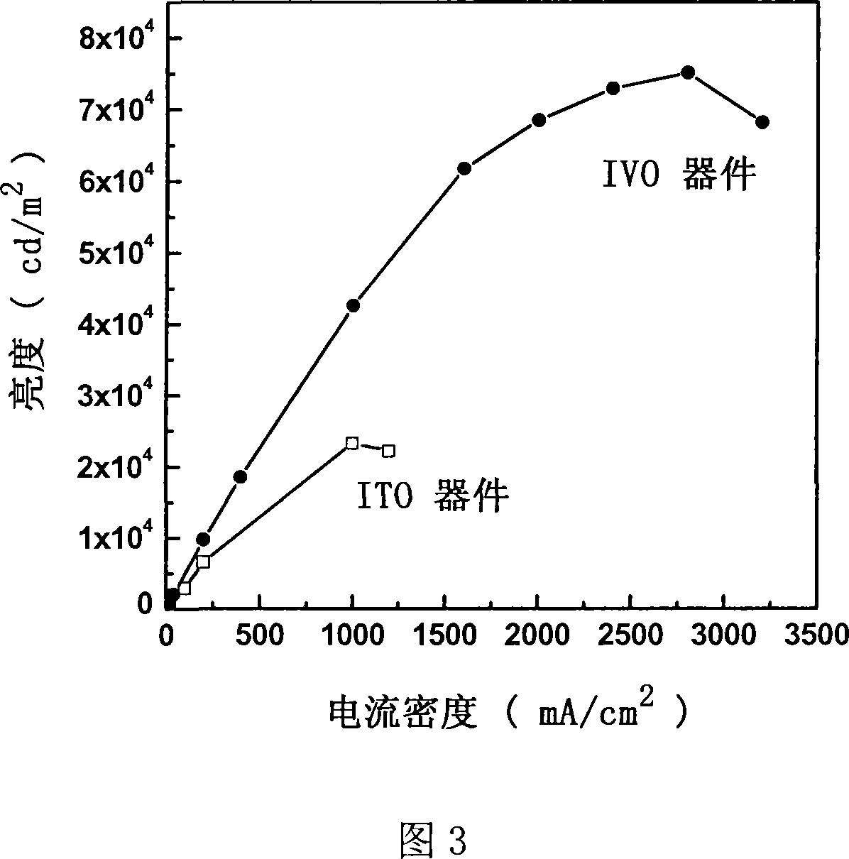
[0037] The ZZS700 box-type high-vacuum coating machine of Chengdu Vacuum Machinery Factory was used to prepare the IVO transparent conductive film by electron beam deposition technology, and the basic technical requirements for vacuum and substrate were the same as in Example 1. First grow a layer of Al on the glass substrate 2 o 3, thick 1 ~ 15nm. Then IVO was prepared on the glass substrate by electron beam thermal evaporation. The evaporation raw material is InV alloy (the mass ratio of metal V to In is 1:3~1:20), and the MDC-360 of MAXTEK Company is used to monitor the growth rate and film thickness of the film in real time. The evaporation rate is 0.05~2nm / s. The mass ratio of V to In after film formation can be 0.1-30% by adjusting the electron beam current and the working vacuum degree. The film thickness ranges from 20nm to 500nm. After the thin film is prepared, the annealing condition is 60-250° C. and the time is 10-300 minutes. Fig. 2 is the scanning electro...

Embodiment 3

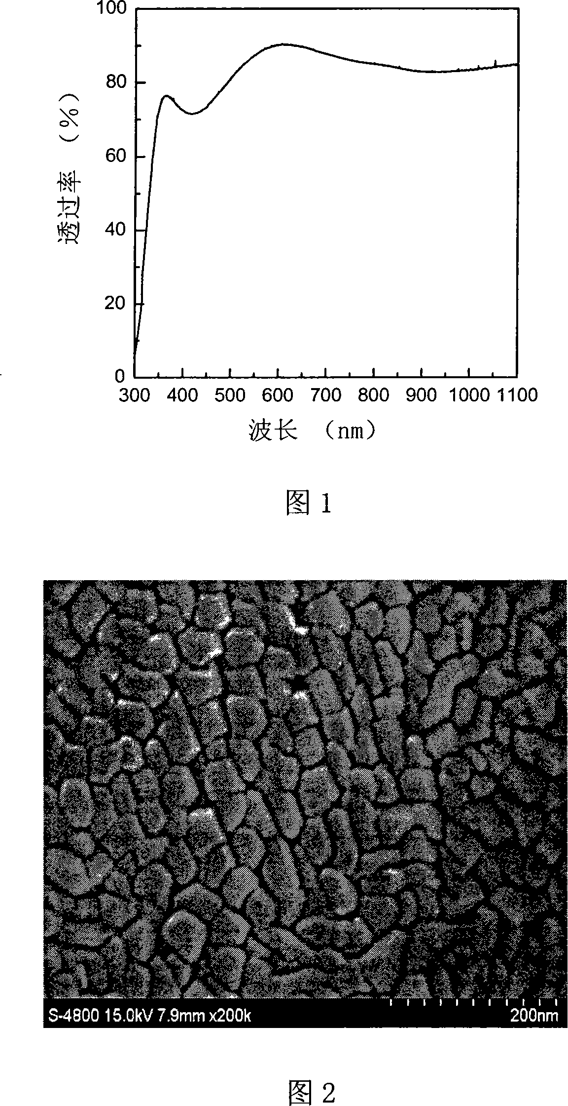
[0039] Using In with a purity of 99.99% 2 o 3 Powder with 99.99% purity V 2 o 5 The powders are evenly mixed with each other (In 2 o 3 with V 2 o 5 The mass ratio is 98:2 to 80:20), and it is sintered into a target material. The target is used to deposit IVO thin film by magnetron sputtering technology. The substrate temperature is 200°C. Sputtering power is radio frequency target 0 ~ 500 watts. The sputtering rate is 0.04-1nm / s. By adjusting sputtering power and working vacuum, the mass ratio of V to In after film formation can be 0.1-30%. The surface resistance of the IVO thin film reaches ~15Ω / □, and the average visible light transmittance is higher than 85%.


PUM

PropertyMeasurementUnit
thicknessaaaaaaaaaa
luminanceaaaaaaaaaa

Abstract

The invention relates to a transparent conductive thin film widely applied in the technical fields such as a LCD screen, an electroluminescent display, a solar cell, a TFT, an organic and inorganic semiconductor laser, and thermal-insulating energy-saving glass, as well as a preparation method thereof. The thin film (IVO) is an indium vanadium oxide (In2O3:V) formed by doping V element in a main material In2O3, and the content of V in the IVO material accounts for 0.1 percent-30 percent of the content of In. The thin film can be prepared by a plurality of film plating techniques such as high vacuum thermal evaporation, electron beam deposition and sputtering. The thin film is firm, and has good conductivity, visible light transparency and chemical stability.

Description

technical field [0001] The invention relates to a transparent conductive film which can be widely used in technical fields such as liquid crystal displays, electroluminescent displays, solar cells, thin film transistors, organic and inorganic semiconductor lasers, heat-insulating and energy-saving glass, and a preparation method thereof. Background technique [0002] The transparent conductive film refers to a film formed on a substrate that is transparent to visible light and can conduct electricity. As an excellent optoelectronic information material, transparent conductive film has high light transmittance and low resistivity in the visible light range. These excellent characteristics make it widely used in technical fields such as liquid crystal display screens, electroluminescent displays, solar cells, thin film transistors, organic and inorganic semiconductor lasers, and heat-insulating and energy-saving glass. For transparent conductive films, indium oxide (Indium ox...

Claims


Application Information

Patent Timeline
Patent Type & Authority Applications(China)
IPC IPC(8): H01B5/14H01B1/08H01B13/00C23C14/24C23C14/08G09F9/30H05B33/28
Inventor 李会斌王宁刘星元
Owner CHANGCHUN INST OF OPTICS FINE MECHANICS & PHYSICS CHINESE ACAD OF SCI
Why Eureka
Try Eureka