Insulating layer upper semiconductor structure with low dielectric constant as insulation buried layer and its method

A technology of low dielectric constant and insulating buried layer, which is applied in semiconductor devices, semiconductor/solid-state device manufacturing, electric solid-state devices, etc. Large equivalent impedance, reduced capacitance, suitable for low noise effects

Inactive Publication Date: 2008-05-07
SHANGHAI INST OF MICROSYSTEM & INFORMATION TECH CHINESE ACAD OF SCI +1
View PDF0 Cites 23 Cited by
  • Summary
  • Abstract
  • Description
  • Claims
  • Application Information

AI Technical Summary

Problems solved by technology

But this method is bound to aggravate the SiO 2 The self-heating effect of the buried layer b

Method used


Image

  • Insulating layer upper semiconductor structure with low dielectric constant as insulation buried layer and its method
  • Insulating layer upper semiconductor structure with low dielectric constant as insulation buried layer and its method
  • Insulating layer upper semiconductor structure with low dielectric constant as insulation buried layer and its method

Examples


Embodiment 1

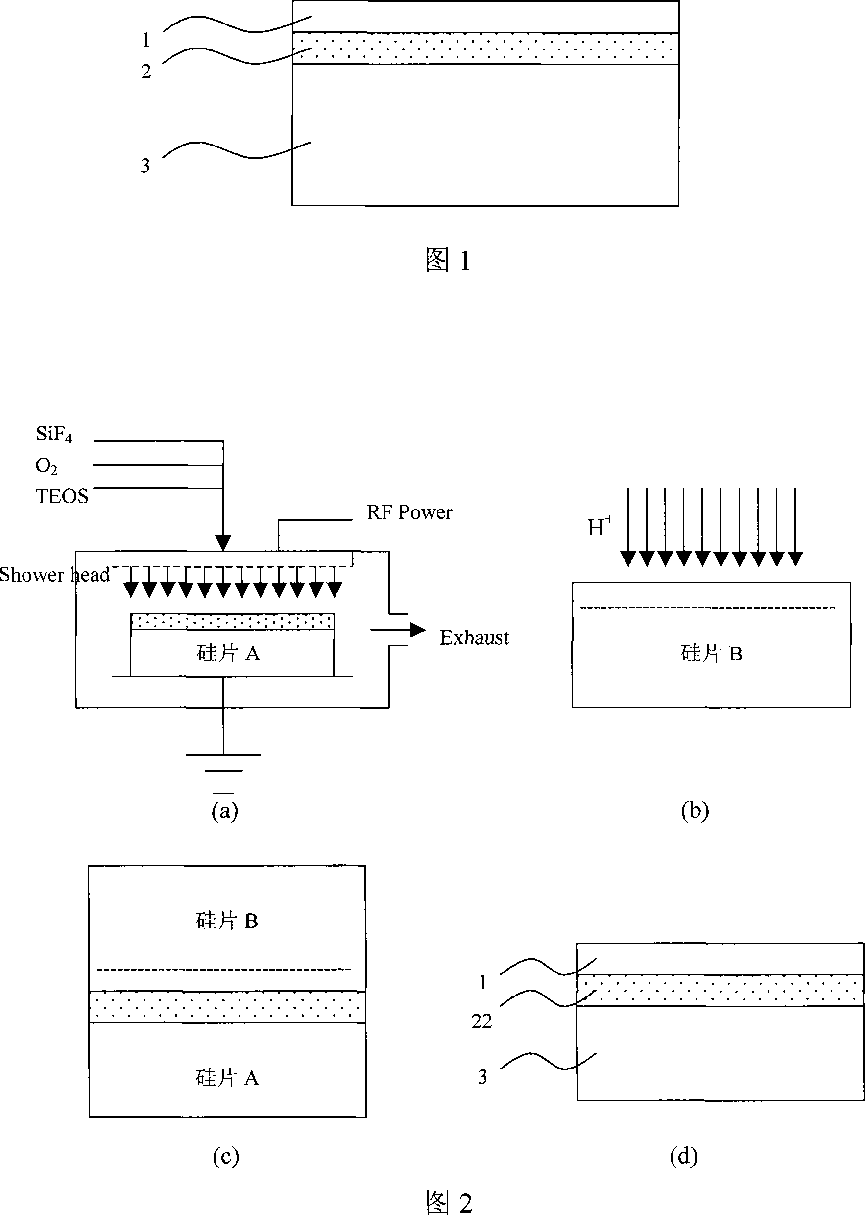
[0038] Embodiment 1: A method for fabricating an SOI structure containing a low dielectric constant SiOF buried layer.

[0039] 1. Using n-type (100) silicon wafer A as the substrate material, SiOF film was prepared by plasma enhanced chemical vapor deposition (PECVD), as shown in Figure 2(a), with TEOS, SiF 4 , O 2 As the raw material, the flow rate is 20sccm, 40sccm, 40sccm respectively, the pressure in the reaction chamber is 90Pa, and the substrate temperature is 400°C;

[0040] 2. In order to ensure the bonding quality, the silicon wafer A deposited with the SiOF film is chemically mechanically polished to reduce the surface roughness to below 1nm;

[0041] 3. Perform H on silicon wafer B + Injection, as shown in Figure 2(b), the injection dose is 6E16cm -2 , the injection energy is 140keV;

[0042]4. The two silicon wafers are bonded by plasma activation at room temperature, as shown in Fig. 2(c). Before bonding, the silicon wafer is cleaned by RCA, and then the sur...

Embodiment 2

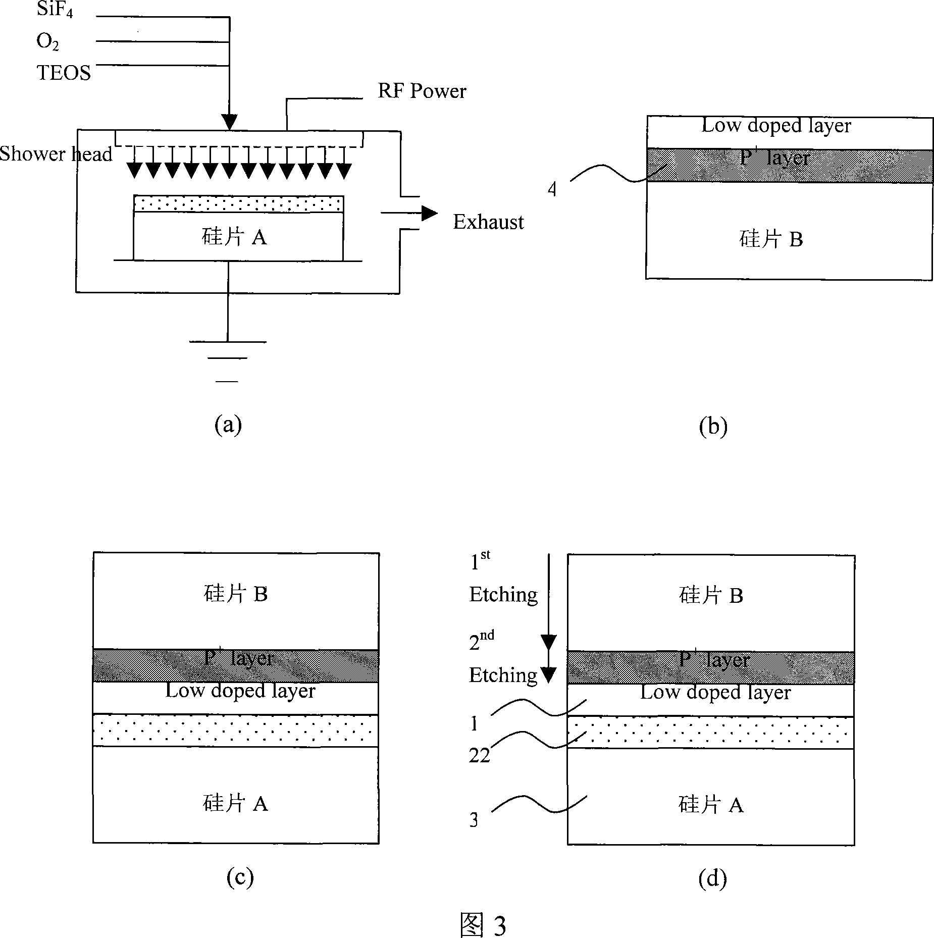
[0045] Embodiment 2: A method for fabricating an SOI structure containing a low dielectric constant SiOF buried layer.

[0046] 1. Using n-type (100) silicon wafer A as the substrate material, SiOF film was prepared by plasma enhanced chemical vapor deposition (PECVD), as shown in Figure 3(a), with TEOS, SiF 4 , O 2 As the raw material, the flow rate is 20sccm, 40sccm, 40sccm respectively, the pressure in the reaction chamber is 90Pa, and the substrate temperature is 400°C;

[0047] 2. In order to ensure the bonding quality, the silicon wafer A deposited with the SiOF film is chemically mechanically polished to reduce the surface roughness to below 1nm;

[0048] 3. Epitaxial layer of 200nm P on silicon wafer B + The silicon layer is used as an etching stop layer, and a 50nm low-doped silicon layer is epitaxially, as shown in Figure 3(b);

[0049] 4. Perform room temperature plasma activated bonding of two silicon wafers, as shown in Figure 3(c). Before bonding, the silicon...

Embodiment 3

[0052] Embodiment 3: A method for preparing an SOI structure of a low dielectric constant SiOF buried layer.

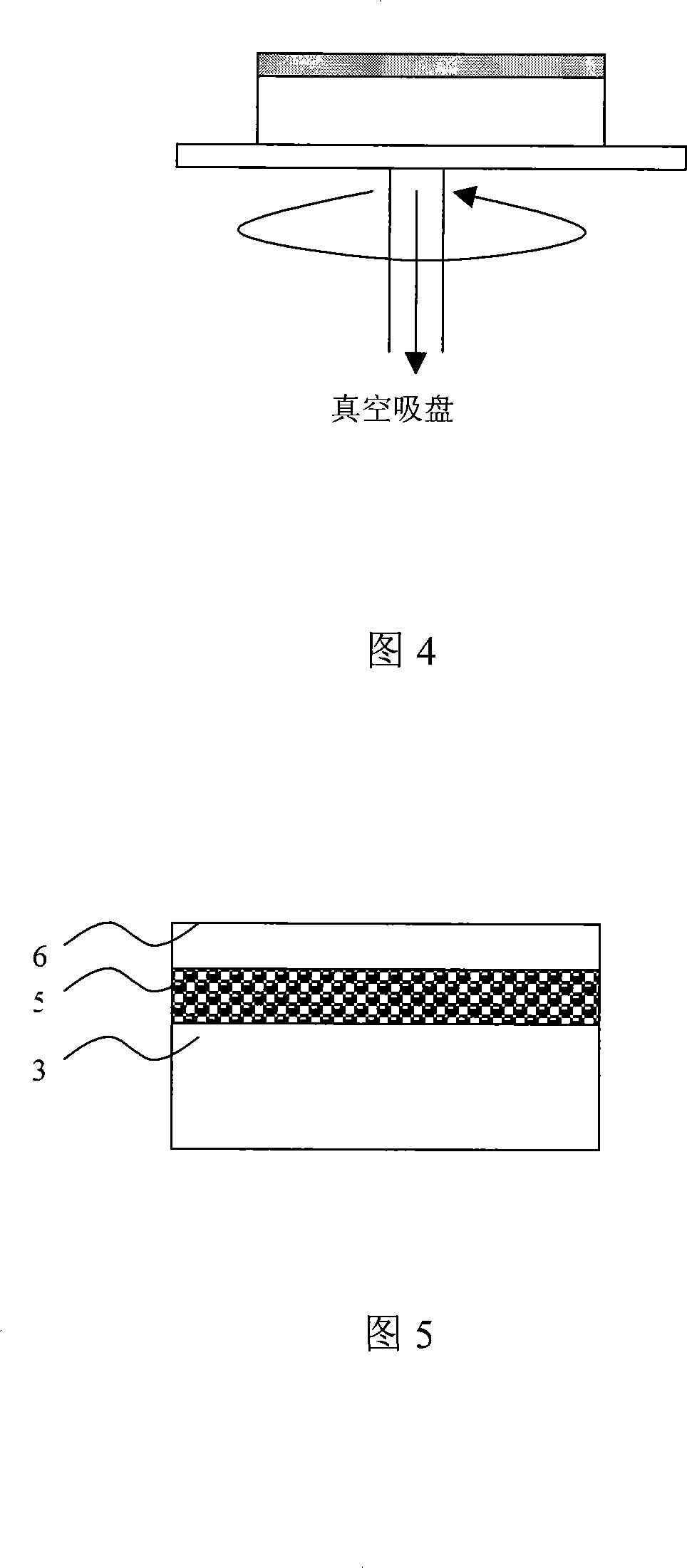
[0053] 1. This example is exactly the same as Example 1, only the SiOF film is prepared by the sol-gel method, and the process parameters and conditions for the preparation. Organic compounds, the precursor solution was spin-coated on the silicon wafer at a spin-coating rate of 2500rpm, and then annealed at 400°C to prepare a SiOF film (Figure 4).


PUM

PropertyMeasurementUnit
Thicknessaaaaaaaaaa
Resistivityaaaaaaaaaa

Abstract

The invention provides a semiconductor structure on an insulation layer with low dielectric constant material as the insulation buried layer and the preparation method thereof, which belongs to the microelectronic semiconductor material and the preparation craft thereof. The invention is characterized in that the structure comprises three layers: a semiconductor layer at the top, an insulation buried layer with the relative dielectric constant being smaller than 4.2 in the middle and a silicon substrate on the lower layer. The preparation is characterized in that low dielectric constant film is prepared on a silicon wafer by utilizing methods such as a chemical vapor deposition method or a sol gel method, then linked with the silicon wafer containing the semiconductor layer, and the transfer of the semiconductor layer at the top is realized by adopting a smart-cut technology or a back grinding technology. The low dielectric constant material is adopted to replace the prior SiO2 buried layer in the silicon (SOI) on the insulation layer, in order to reduce the capacitance of the insulation buried layer, thus increasing the equivalent impedance (1/2 Pi fC) of the buried layer under high frequency, therefore, compared with the prior SOI substrate material, the invention can reduce the signal crosstalk via the substrate under high frequency, thereby being more suitable for the requirement of a low-noise SOI circuit.

Description

Background technique [0001] With the rapid development of the wireless communication field, the system on chip (system on chip, SOC) is becoming the mainstream technology, BiCMOS (Bipolar Complementary Metal Oxide Semiconductor, Bipolar Complementary Metal Oxide Semiconductor), as an advanced technology for realizing SOC, makes the bipolar Circuits and CMOS circuits are integrated on the same chip, which has the characteristics of high density, low power consumption and high speed. In order to avoid the impact of noise injected into the substrate by MOS (Metal Oxide Semiconductor) devices on Bipolar bipolar devices, it is a good choice to use SOI substrates. The combination of SOI substrates and deep groove technology can provide Complete dielectric isolation between devices. However, there is an upper frequency limit for traditional SOI substrates to block noise: when the signal frequency is low, high-impedance SiO 2 The buried layer can effectively prevent the passage of n...

Claims


Application Information

Patent Timeline
IPC IPC(8): H01L27/12H01L29/786H01L21/00H01L21/02H01L21/20H01L21/762H01L21/84H01L21/336
Inventor 陈超刘卫丽宋志棠林成鲁
Owner SHANGHAI INST OF MICROSYSTEM & INFORMATION TECH CHINESE ACAD OF SCI
Why Eureka
Try Eureka