GaN dual heterogeneity node field effect transistor structure and its making method

A field effect transistor, gallium nitride based technology, applied in the fields of semiconductor/solid state device manufacturing, semiconductor devices, electrical components, etc. Adverse effects of electron gas transport properties, difficulties in epitaxial growth, etc., to reduce electron scattering, suppress current collapse effect, and improve mobility

Inactive Publication Date: 2008-09-17
INST OF SEMICONDUCTORS - CHINESE ACAD OF SCI
View PDF0 Cites 16 Cited by
  • Summary
  • Abstract
  • Description
  • Claims
  • Application Information

AI Technical Summary

Problems solved by technology

[0005] Before the present invention, in order to increase the barrier height of the buffer layer, the (In)GaN channel double heterojunction field effect transistor structure usually grows the channel layer on the AlGaN buffer layer, which is comparable to the GaN buffer layer. Compared with AlGaN and the substrate (sapphire, silicon carbide, silicon), there is a larger lattice mismatch, and it is difficult to directly epitaxially produce a high-quality AlGaN buffer layer on the substrate. Therefore, it is necessary to Under the AlGaN layer, a thick GaN buffer layer is first grown as a transition layer, resulting in the formation of additional conductive channels at the interface between the AlGaN buffer layer and the thick GaN layer, which affects the performance of the device; at the same time, the AlGaN As a ternary alloy, the crystal quality is poor, and the interface alloy disorder and roughness scattering will adversely affect the transport performance of the channel two-dimensional electron gas
Therefore, there is currently a double heterogeneous field effect transistor structure. Through the introduction of the AlGaN buffer layer, although the barrier height on one side of the buffer layer is increased, and the confinement effect of the buffer layer on the two-dimensional electron gas of the channel is enhanced, but At the same time, the epitaxial growth is more difficult. Under the current process conditions, it is difficult to obtain high-quality (indium) gallium nitrogen channel double heterojunction field effect transistor structure materials, which leads to the current double heterojunction field effect transistor structure. The important reason for taking advantage of this structure requires further measures to further optimize the design of the double heterojunction field effect transistor structure

Method used


Image

  • GaN dual heterogeneity node field effect transistor structure and its making method
  • GaN dual heterogeneity node field effect transistor structure and its making method
  • GaN dual heterogeneity node field effect transistor structure and its making method

Examples


Embodiment Construction

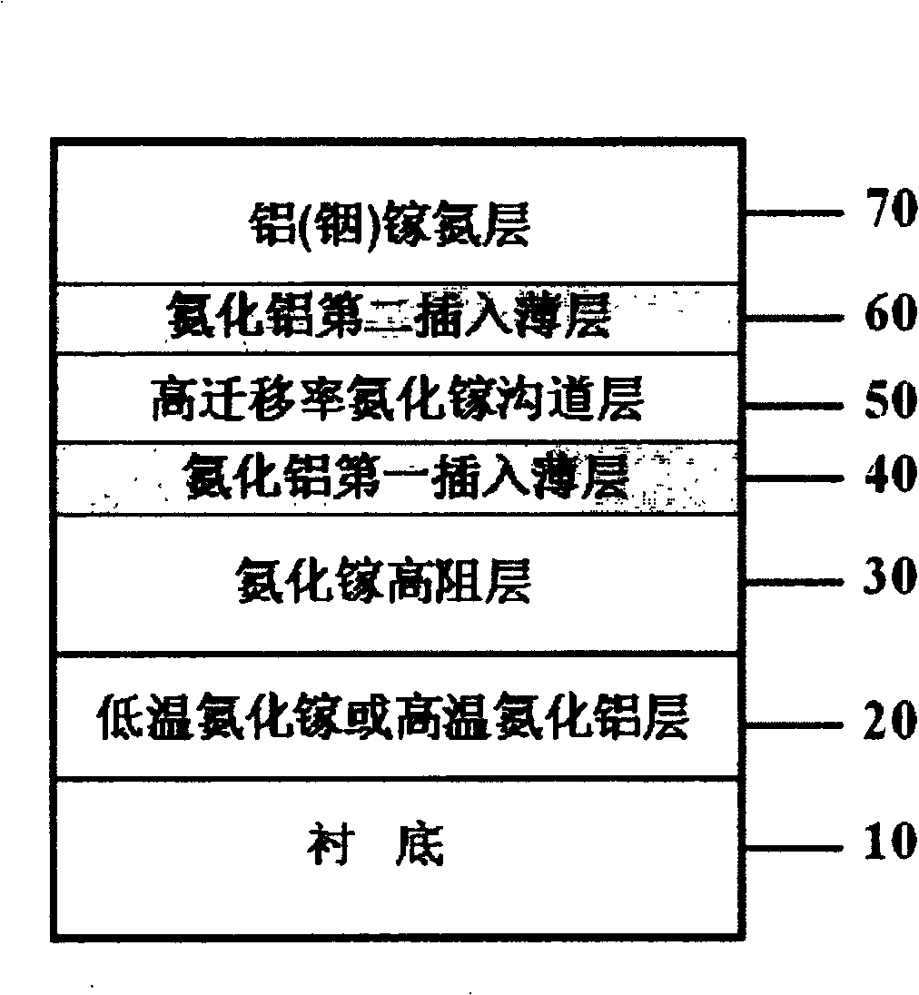
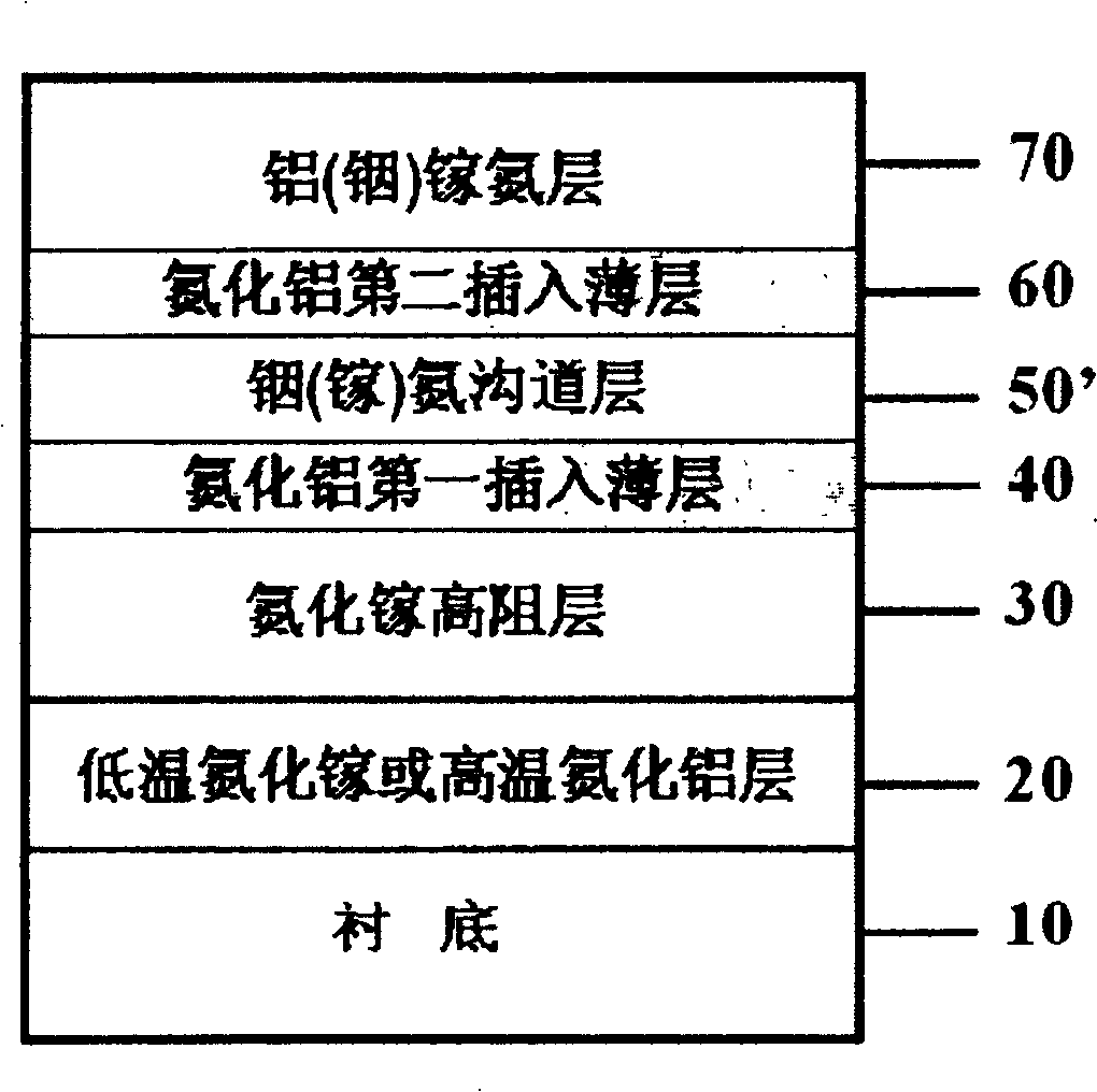
[0059] The present invention is a gallium nitride-based double heterojunction field effect transistor structure using a double aluminum nitride insertion layer. Between the channel layer and the aluminum (indium) gallium nitride barrier layer, and between the gallium nitride-based channel layer and the gallium nitride high-resistance buffer layer, insert thin layers of aluminum nitride to form a double heterogeneous field effect Transistor structure, through precise control of growth conditions, such as temperature, pressure, V / III ratio, high-quality gallium nitride-based double heterojunction field effect transistor structure materials are grown. Double aluminum nitride inserted into the thin layer can further increase the barrier height on both sides of the channel layer, which can better confine the two-dimensional electron gas in the channel layer, and effectively limit the flow of electrons to the aluminum (indium) gallium nitrogen barrier. layer and GaN buffer layer lea...


PUM

PropertyMeasurementUnit
thicknessaaaaaaaaaa
thicknessaaaaaaaaaa
electrical resistivityaaaaaaaaaa

Abstract

A gallium nitride-based double heterojunction field effect transistor structure comprises a substrate, a low temperature gallium nitride layer or high temperature aluminum nitride layer formed on the substrate; a high insulation layer with unintentional-doped or doped gallium nitride; the high insulation layer with unintentional-doped or doped gallium nitride is formed on a low temperature gallium nucleation layer or a high temperature gallium nitride nucleation layer; a first aluminum nitride inserting layer, the first aluminum nitride inserting layer is formed on the high insulation layer with unintentional-doped or doped gallium nitride; a unintentional-doped gallium nitride channel layer, the unintentional-doped gallium nitride channel layer is formed on the first aluminum nitride inserting layer; a second aluminum nitride inserting layer, the second aluminum nitride inserting layer is formed on the unintentional-doped gallium nitride channel layer, an unintentional-doped or n-type doped AlxInyGazN layer, the unintentional-doped or n-type doped AlxInyGazN layer is formed on the second aluminum nitride inserting layer.

Description

technical field [0001] The invention belongs to the field of semiconductor technology, in particular to a gallium nitride-based double heterojunction field-effect transistor structure and a manufacturing method using a double aluminum nitride insertion layer, which can significantly improve the transport performance of the two-dimensional electron gas of the material, Effectively limit the leakage of channel electrons to the barrier layer and buffer layer, suppress the current collapse effect and improve the two-dimensional electron gas mobility of the channel. Background technique [0002] As a typical representative of the third-generation wide-bandgap semiconductor, gallium nitride has excellent thermal and chemical stability, high breakdown voltage, high electron saturation drift velocity and excellent radiation resistance, and is especially suitable for the preparation of high temperature, high Heterojunction field effect transistors with high frequency, high power and ...

Claims


Application Information

Patent Timeline
Patent Type & Authority Applications(China)
IPC IPC(8): H01L29/778H01L21/335
Inventor 王晓亮马志勇冉学军肖红领王翠梅胡国新唐健罗卫军
Owner INST OF SEMICONDUCTORS - CHINESE ACAD OF SCI
Why Eureka
Try Eureka