Internal heating oxidation method for preparing silicon material on isolator

A silicon-on-insulator, internal heat technology, used in semiconductor/solid-state device manufacturing, electrical components, circuits, etc., can solve the problems of low thermal oxidation efficiency, long annealing time, unsuitable for industrial production, etc., to improve quality and accelerate nucleation. and growth, the effect of reducing stress

Active Publication Date: 2009-03-18
SHANGHAI SIMGUI TECH +1
View PDF0 Cites 2 Cited by
  • Summary
  • Abstract
  • Description
  • Claims
  • Application Information

AI Technical Summary

Problems solved by technology

[0005] The disadvantage of the existing technology is that the efficiency of internal thermal oxidation is very low, resulting in most of the top silicon being oxidized, and the annealing time in the internal thermal oxidation process is too long, which is not suitable for industrial production

Method used


Image

  • Internal heating oxidation method for preparing silicon material on isolator
  • Internal heating oxidation method for preparing silicon material on isolator
  • Internal heating oxidation method for preparing silicon material on isolator

Examples


preparation example Construction

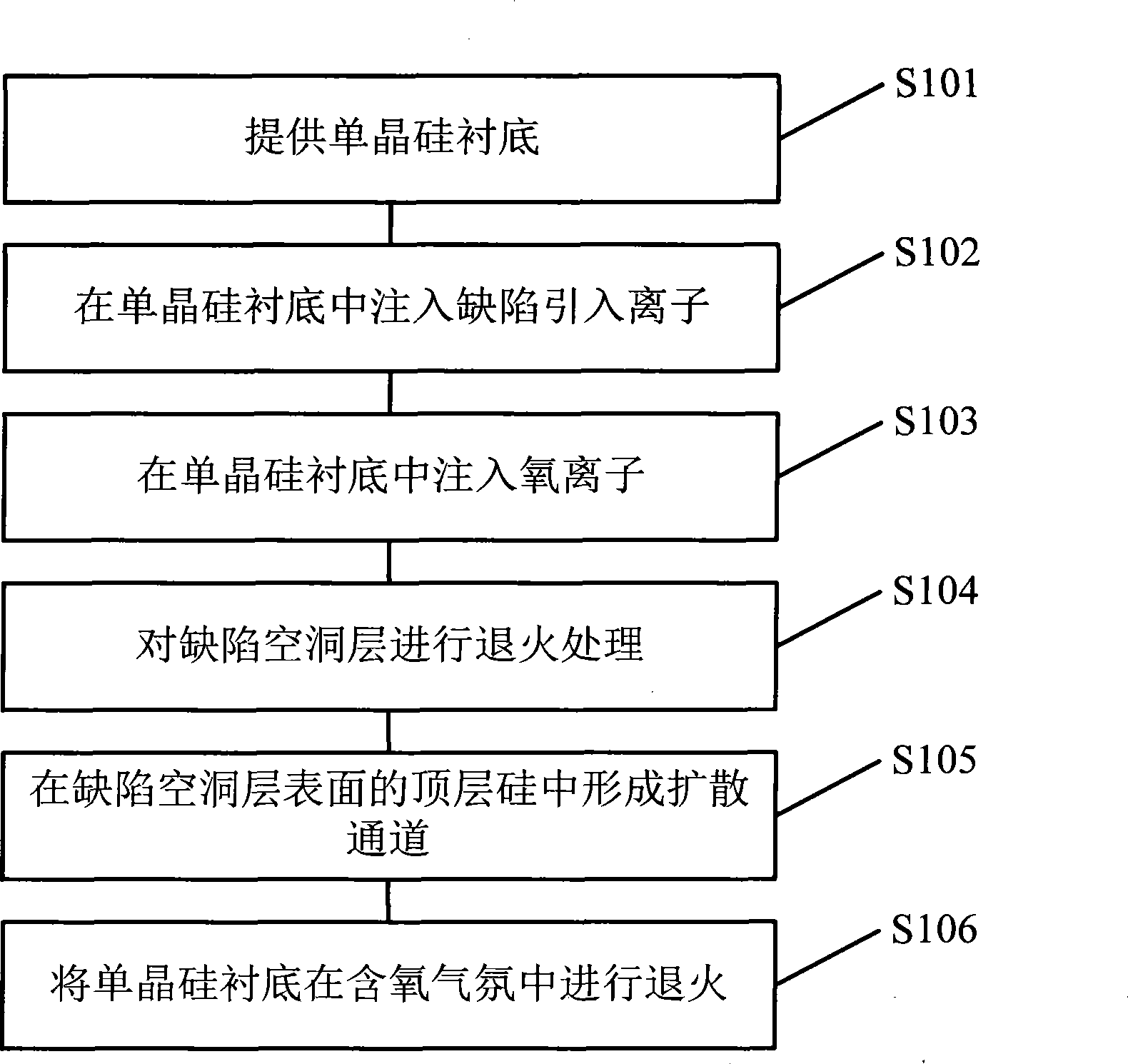
[0022] The specific implementation of the internal thermal oxidation method for preparing a silicon-on-insulator material provided by the present invention will be described in detail below in conjunction with the accompanying drawings.

[0023] attached figure 1 Shown is the flow chart of the implementation steps of this specific embodiment, including the following steps: step S101, providing a single crystal silicon substrate; step S102, implanting defect-introducing ions into the single crystal silicon substrate, so that the single crystal silicon substrate Forming a defect hole layer and a top layer of silicon on the surface of the defect hole layer; step S103, implanting oxygen ions into the single crystal silicon substrate; step S104, performing annealing treatment on the defect hole layer; step S105, forming the top layer on the surface of the defect hole layer Diffusion channels are formed in the silicon; step S106 , annealing the single crystal silicon substrate in an...

Embodiment 1

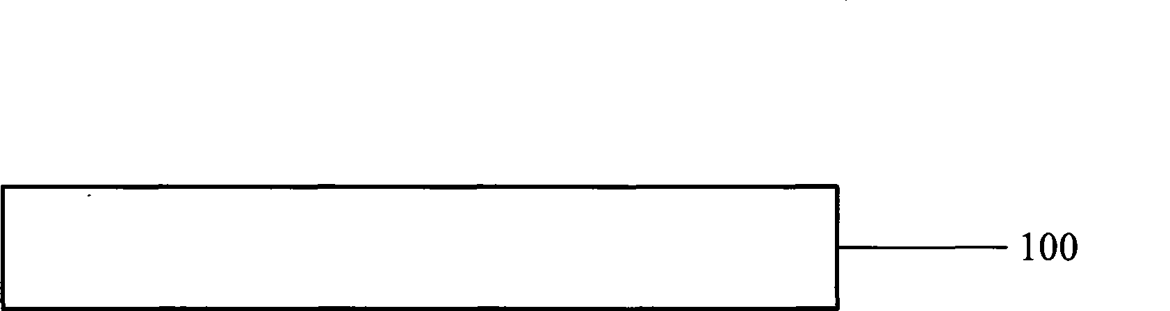
[0057] 1. Provide a single crystal silicon substrate.

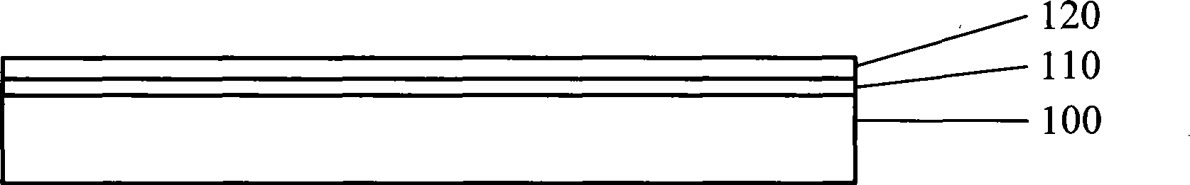
[0058] 2. At room temperature, helium ions were implanted into the single crystal silicon substrate with a dose of 4×10 16 cm -2 , the energy is 45keV, and a defect cavity layer is formed, and the depth of the defect cavity layer is at 0.35 μm. attached Figure 7 Shown is a transmission electron micrograph of the defect-cavity layer.

[0059] 3. Anneal at 1000°C for 1 hour.

[0060] 4. Through SiO2 2 Template shadowing and Ga + Diffusion grooves with a width of 2 μm and a depth of 0.5 μm were etched on the silicon layer above the defect hole layer by ion etching, and the distance between the grooves was 5 μm. attached Figure 8 Shown is a scanning electron micrograph of the surface topography of the top silicon layer after etching.

[0061] 5. In the pure oxygen annealing atmosphere, keep the temperature at 1200°C for 20 minutes, then raise the temperature to 1340°C in the annealing atmosphere with a gas concentra...

Embodiment 2

[0064] 1. Provide a single crystal silicon substrate.

[0065] 2. At room temperature, implant hydrogen ions into the single crystal silicon substrate with a dose of 2×10 16 cm -2 , the energy is 40keV, forming a defect hole layer.

[0066] 3. Implant the silicon wafer with the defect hole layer at room temperature with a dose of 1×10 15 cm -2 , the energy is 150keV, at this time an amorphous silicon layer is formed on the upper interface of the void layer, and the maximum concentration of oxygen distribution is located in the void layer.

[0067] 4. In an annealing atmosphere with a gas concentration ratio of oxygen and argon of 100:2 and a temperature of 1340°C, keep the temperature for 5 hours.

[0068] 5.10% HF solution corrodes the surface SiO 2 layer.


PUM


Abstract

The invention relates to an internal thermal oxidation process for preparing silicon material on an insulator, which comprises the following steps: providing a single-crystal silicon substrate, implanting defect introducing ions into the single-crystal silicon in order to form a defect void layer in the single-crystal substrate and top silicon on the surface of the defect void layer, forming diffusion channels in the top silicon on the surface of the defect void layer, and conducting annealing for the single-crystal silicon substrate in oxygen-containing atmosphere. The invention has the advantages that defect introducing irons are implanted into the single-crystal silicon substrate to form the defect void layer, and the defect void layer used as a silicon oxide aggregate nucleation can provide the nucleation center with high density, thereby accelerating the formation and the growth of the silicon oxide aggregate, and reducing or completely replacing the implanted oxygen dosage in a continuous silicon dioxide insulating layer formed by the technology of separation by implanted oxygen (SIMOX). Simultaneously, the void volume in the defect void layer can absorb the volume expansion effect generated by the formation of the silicon oxide aggregate, reduces the stress of the top silicon with a BOX layer interface, and increases the quality of SOI material.

Description

【Technical field】 [0001] The invention relates to a method for preparing integrated circuit materials, in particular to an internal thermal oxidation method for preparing silicon-on-insulator materials. 【Background technique】 [0002] Silicon-on-insulator (SOI, Silicon-on-insulator) technology is considered to be the key technology to continue the development speed of Moore's Law in the manufacture of submicron ultra-large integrated circuits, and has attracted much attention from academic and industrial circles at home and abroad. As the basis of SOI technology development, SOI materials have developed rapidly over the past 10 years with the demand for high-speed, low power consumption, and radiation-resistant microelectronic devices in the fields of ultra-large integrated circuits, aviation, aerospace and national defense, and portable communications. A new type of microelectronic material. [0003] Oxygen injection isolation technology SIMOX (Seperation-implantation-by-o...

Claims


Application Information

Patent Timeline
Patent Type & Authority Applications(China)
IPC IPC(8): H01L21/00H01L21/20H01L21/316H01L21/265H01L21/762H01L21/84
Inventor 欧欣王曦张苗
Owner SHANGHAI SIMGUI TECH
Why Eureka
Try Eureka