Substrate for flexible organic optoelectronic device and preparation method thereof

A technology for optoelectronic devices and substrates, which is applied in the fields of electrical solid-state devices, semiconductor/solid-state device manufacturing, photovoltaic power generation, etc., and can solve problems such as poor adhesion between thin films and substrates

Inactive Publication Date: 2009-06-24
UNIV OF ELECTRONIC SCI & TECH OF CHINA
View PDF0 Cites 59 Cited by
  • Summary
  • Abstract
  • Description
  • Claims
  • Application Information

AI Technical Summary

Problems solved by technology

[0007] The technical problem to be solved by the present invention is how to provide a substrate for flexible organic optoelectronic devices and its preparation method, which solves the problem of poor adhesion between the deposited film and the substrate due to the low surface energy of the flexible

Method used


Image

  • Substrate for flexible organic optoelectronic device and preparation method thereof
  • Substrate for flexible organic optoelectronic device and preparation method thereof
  • Substrate for flexible organic optoelectronic device and preparation method thereof

Examples


Embodiment 1

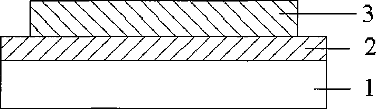
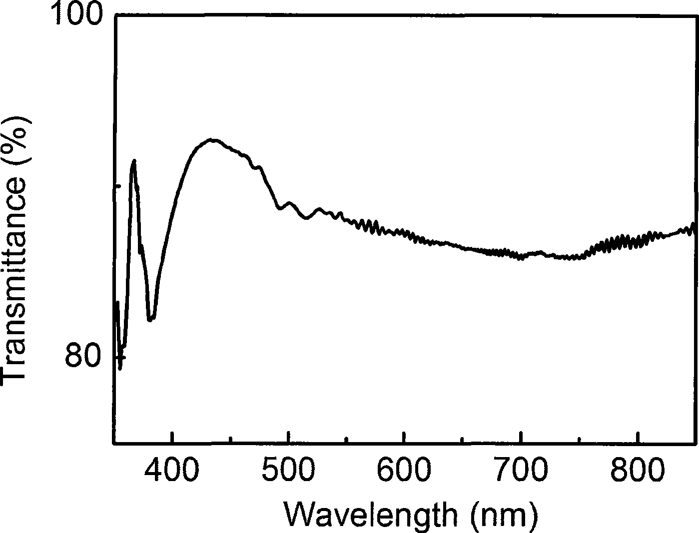
[0157] Such as figure 1 As shown in the substrate structure, the flexible substrate 1 adopts a flexible polyethylene terephthalate polymer (PET) substrate, and the adhesive layer 2 adopts a single-layer free radical UV curing agent-isocyanate thermal curing agent dual curing system, which is electrically conductive. Film 3 is a DC magnetron sputtered ITO transparent conductive film. The transmittance test curve is as figure 2 shown.

[0158] The preparation method is as follows:

[0159] ①Use detergent, acetone solution, ethanol solution and deionized water to ultrasonically clean the PET substrate, and dry it with dry nitrogen after cleaning;

[0160] ② Stir the adhesive diluted 1:10 with ethanol for 20 hours, then spin-coat on the PET surface at a speed of 2000 rpm for one minute, and the film thickness is about 100 nanometers;

[0161] Wherein the ratio of adhesive raw material components is:

[0162] Acrylic resin (free radical UV curing agent) 30-40 parts

[0163] ...

Embodiment 2

[0173] Such as figure 1 As shown in the substrate structure, the flexible substrate 1 is a flexible metal foil substrate, the adhesive layer 2 is a dual curing system of a single-layer free radical UV curing agent-epoxy resin thermal curing agent, and the conductive film 3 is DC magnetron sputtering. ITO transparent conductive film.

[0174] The preparation method is as follows:

[0175] ①Use detergent, acetone solution, ethanol solution and deionized water to ultrasonically clean the PET substrate, and dry it with dry nitrogen after cleaning;

[0176] ② Stir the adhesive diluted 1:10 with ethanol for 20 hours, then spin-coat on the surface of the flexible metal foil substrate at a speed of 2000 rpm for one minute, and the film thickness is about 100 nanometers;

[0177] Wherein the ratio of adhesive raw material components is:

[0178] Unsaturated polyester resin (free radical UV curing agent) 30-40 parts

[0179] Epoxy resin (heat curing agent) 35~45 parts

[0180] Mult...

Embodiment 3

[0189] Such as figure 1 As shown in the substrate structure, the flexible substrate 1 adopts a flexible PET substrate, the adhesive layer 2 adopts a single-layer epoxy cationic UV curing agent-amino resin thermal curing agent dual curing system, and the conductive film 3 is a polymer PEDOT:PSS conductive film.

[0190] The preparation method is as follows:

[0191] ①Use detergent, acetone solution, ethanol solution and deionized water to ultrasonically clean the PET substrate, and dry it with dry nitrogen after cleaning;

[0192] ② Stir the adhesive diluted 1:10 with ethanol for 20 hours, then spin-coat on the PET surface at a speed of 2000 rpm for one minute, and the film thickness is about 100 nanometers;

[0193] Wherein the ratio of adhesive raw material components is:

[0194] Epoxy resin (cationic UV curing agent) 35-45 parts

[0195] Amino resin (thermal curing agent) 40-45 parts

[0196] Thinner (vinyl ether monomer) 4.0~9 parts

[0197] Cationic photoinitiator (...


PUM


Abstract

The invention discloses a flexible substrate used for optoelectronic devices and comprises a flexible substrate; the invention is characterized in that a bonding layer and a conductive thin film are arranged on the surface of the flexible substrate; the conductive thin film is deposited on the surface of the bonding layer; and the material of the bonding layer is an adhesive with a double-curing system comprising UV curing-thermal curing or UV curing-microwave curing or UV curing-anaerobic curing or UV curing-electron beam curing. The substrate solves the problem of poor adhesion between the deposited conductive thin film and the substrate due to low surface energy of the flexible substrate and improves the barrier properties of the substrate on water and oxygen, and also achieves good smoothing effect on the surface of the substrate; besides, the preparation method is simple and effective, which can significantly reduce the substrate production cost and process difficulty and increase the substrate yield rate in the etching process.

Description

technical field [0001] The invention relates to the technical field of organic optoelectronic devices, in particular to a flexible organic optoelectronic device substrate and a preparation method thereof. Background technique [0002] Optoelectronics technology is a high-tech industry that develops rapidly after microelectronics technology. With the rapid development of optoelectronic technology, optoelectronic products such as solar cells, optical image sensors, plasma flat panel displays, electroluminescent displays, thin film transistors, and liquid crystal display panels have gradually matured, and they have greatly improved human life. At the same time, the wide application of optoelectronic information technology in various fields of social life has also created a huge growing market. Developed countries regard the optoelectronic information industry as one of the key development areas, and the competition in the optoelectronic information field is unfolding worldwide...

Claims


Application Information

Patent Timeline
IPC IPC(8): H01L51/00H01L51/44H01L51/46H01L51/48H01L51/52H01L51/54H01L51/56C09J167/06C09J4/00C09J163/00C09J161/20C09J163/10
CPCY02E10/50Y02E10/549
Inventor 于军胜李璐蒋亚东钱锦城
Owner UNIV OF ELECTRONIC SCI & TECH OF CHINA
Why Eureka
Try Eureka