
Preparation of yellow copper CIG selenide or sulfide semiconductor thin film material

A technology of chalcopyrite and thin-film materials, which is applied in the field of preparation of selenide or sulfide semiconductor thin-film materials, can solve the problems of little improvement in selenization or vulcanization effect, difficulty in controlling the partial pressure atmosphere, and high post-selenization temperature. Achieve the effects of improving selenization/sulfurization efficiency, saving material consumption, and shortening production time

Inactive Publication Date: 2009-07-08
泉州创辉光伏太阳能有限公司
View PDF2 Cites 11 Cited by
  • Summary
  • Abstract
  • Description
  • Claims
  • Application Information

AI Technical Summary

Problems solved by technology

The disadvantages of the solid source selenization or vulcanization process are: (1) when the solid selenium source is heated in a vacuum chamber to generate saturated selenium vapor, most of the gaseous selenium is converted to Se 5 、Se 6 、Se 7 exist in the form of macromolecular groups or atomic clusters, and H 2 Se is heated and decomposed into monoatomic Se and Cu, In, Ga metal atom reaction situation compares, the condition of the reaction process of macromolecular group selenium or atomic cluster selenium is harsher and complicated; (2) promote macromolecular group selenium or atomic cluster The post-selenization temperature of selenium and Cu, In, Ga metal atoms is very high after the gradual reaction, almost reaching the softening point of the substrate material glass; (3) It is difficult to control the constant partial pressure atmosphere, resulting in the inhomogeneity of the absorption layer
However, this gas-solid contact reaction generates H 2 The effective content of Se is usually less than 2%, and most of it is H 2 And the mixture of selenium (sulfur), the actual selenization or vulcanization effect is not much better than that of solid source selenium (sulfur)

Method used


Image

  • Preparation of yellow copper CIG selenide or sulfide semiconductor thin film material
  • Preparation of yellow copper CIG selenide or sulfide semiconductor thin film material

Examples


Embodiment 1

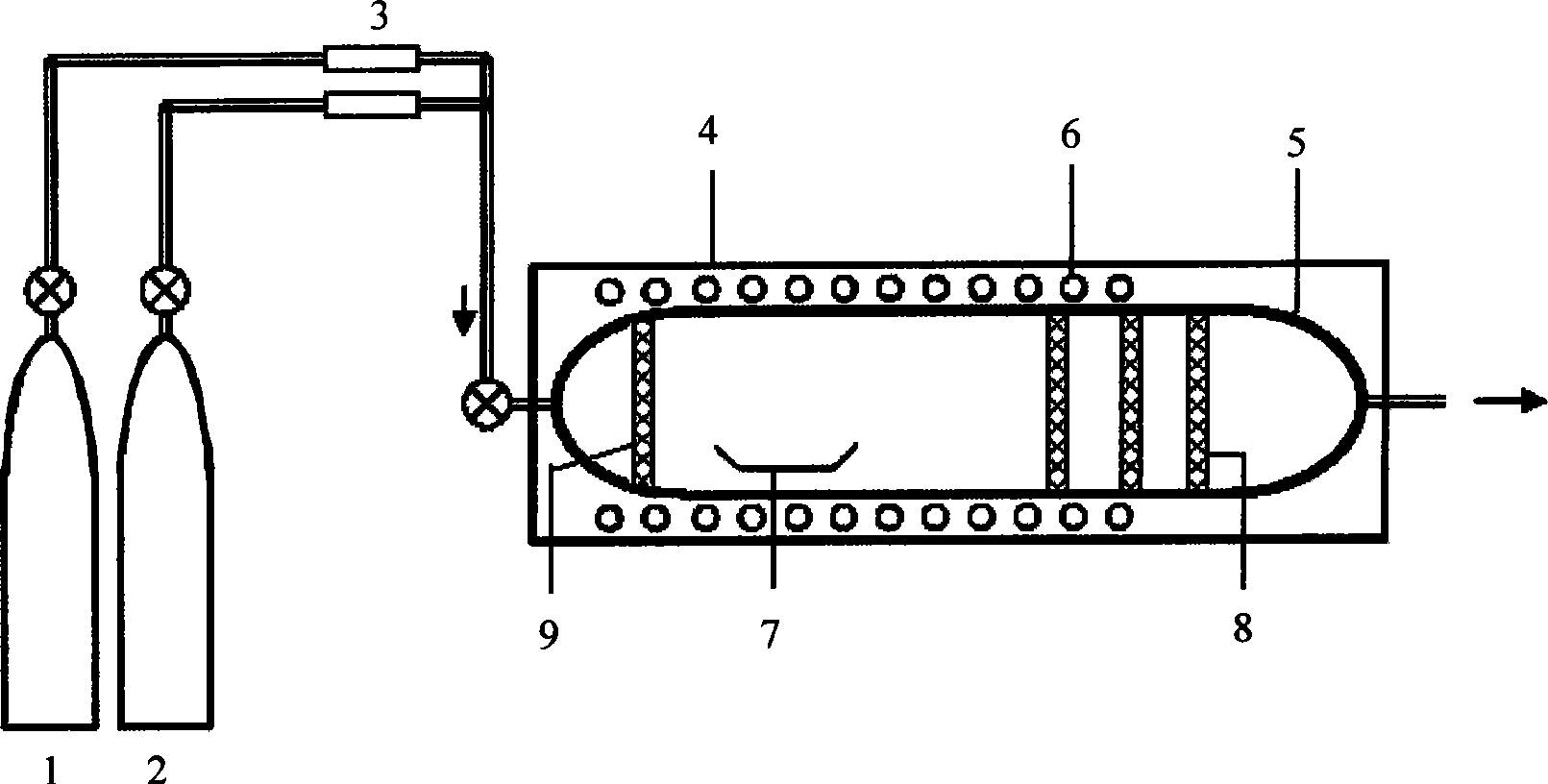
[0031] figure 1 Provide the structural representation of the gas-solid reaction chamber that the embodiment of the present invention adopts, wherein: 1—N 2 / Ar gas source, 2—H 2 Gas source, 3—mass flow meter MFC, 4—stainless steel outer body, 5—gas-solid reaction chamber, 6—resistance heating wire, 7—selenium (sulfur) evaporation source, 8—end heating wire mesh, 9—front heat silk screen.

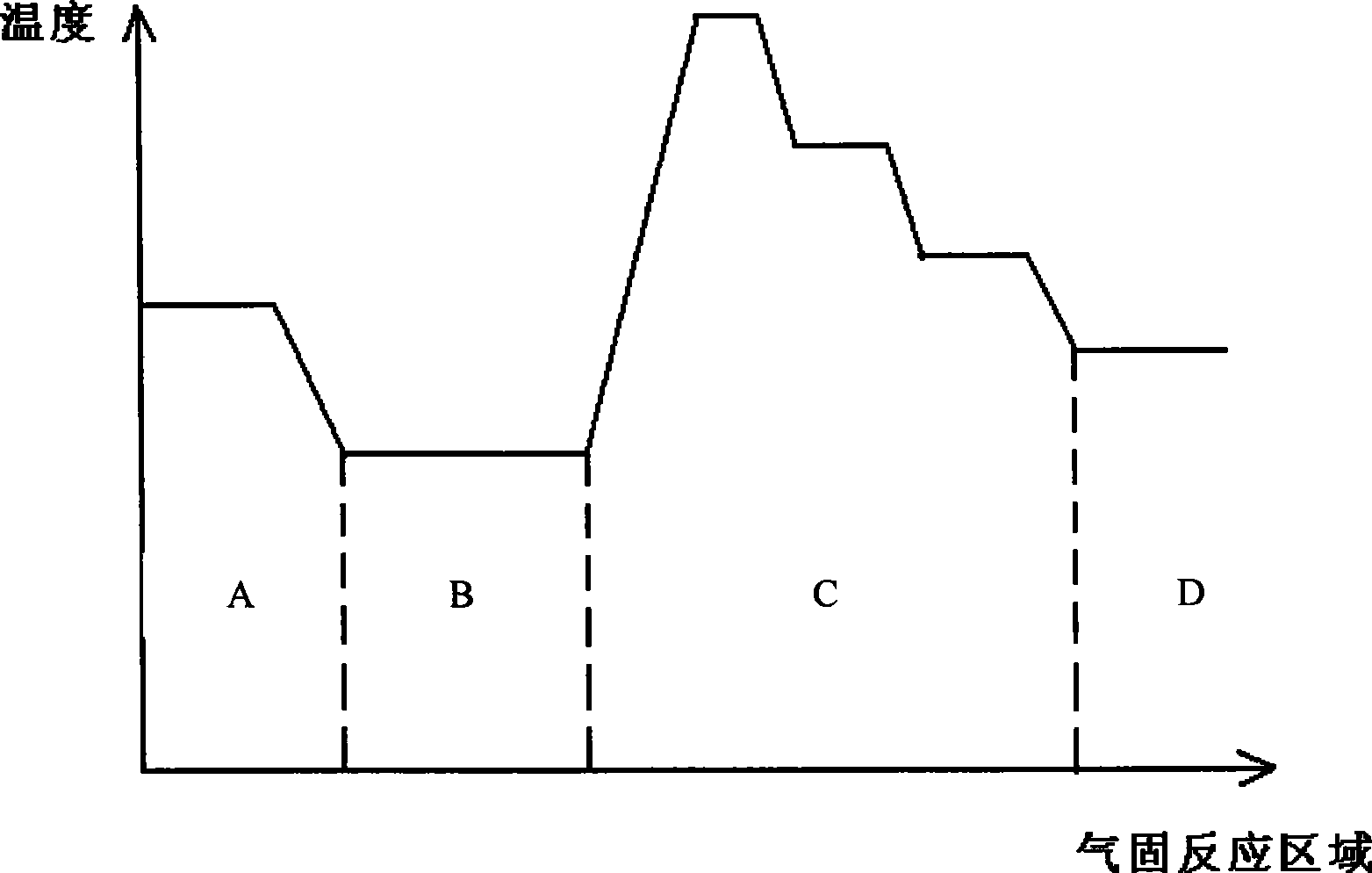
[0032] First use vacuum magnetron sputtering, heating evaporation or chemical water bath electrodeposition method to deposit Cu, In and Ga metal prefabricated layers with chemical formula ratio step by step on the soda lime glass Mo substrate, and then put it into the selenization / sulfurization reaction furnace . Use a vacuum pump to pre-pump the gas-solid reaction chamber and the selenization / sulfurization reaction furnace. After reaching the preset vacuum degree, close each valve. Connect all heating systems in the system, specifically: (1) heat the CIG metal prefabricated layer to 500...


PUM


Abstract

The invention discloses a method for preparing a chalcopyrite-type copper indium gallium selenide or sulfide semiconductor film material and relates to a semiconductor film material. The invention provides a method for preparing the chalcopyrite-type copper indium gallium selenide or sulfide semiconductor film material. A Cu metal prefabricated layer, a In metal prefabricated layer and a Ga metal prefabricated layer are deposited on a soda lime glass Mo substrate by stages through a vacuum magnetron sputtering, heating evaporation or chemical water bath electrodeposition method; N2 and H2 or Ar and H2 are mixed to obtain mixed gas; the mixed gas is introduced to a gas-solid reaction chamber; the reaction chamber is divided into two regions; a solid selenium(sulphur) sublimation region ensures that H2 / N2 (or H2 / Ar) gas and selenium(sulphur) steam are mixed; a hot wire catalytic gas-solid reaction region ensures that H2 and the selenium(sulphur) steam react to generate gaseous H2Se / Se(or H2S / S) mixed atmosphere; and the mixed atmosphere and the Cu metal prefabricated layer, the In metal prefabricated layer and the Ga metal prefabricated layer have thermal selenizing reaction and / or vulcanizing reaction.

Description

technical field [0001] The invention relates to a semiconductor thin film material, in particular to a preparation method of a chalcopyrite copper indium gallium selenide or sulfide semiconductor thin film material. Background technique [0002] Chalcopyrite copper indium selenide (CuInSe 2 , abbreviated as CIS) series solar cells are one of the most efficient and promising thin-film solar cells among various thin-film solar cells, and its composition includes CuInSe 2 、Cu(In,Ga)Se 2 、CuInS 2 , CuIn(S, Se) 2 、Cu(In,Ga)S 2 etc., copper indium gallium selenide (Cu(In, Ga)Se 2 , abbreviated as CIGS) stands for copper indium selenium (CIS) thin film solar cells with higher open circuit voltage Voc and high photoelectric conversion efficiency, which is different from traditional CIS thin film solar cells. Copper indium gallium selenide (CIGS) solar cell is a photovoltaic device formed by depositing multi-layer films on ordinary soda lime glass or polyimide film, metal sheet...

Claims


Application Information

Patent Timeline
IPC IPC(8): C03C17/23
Inventor 吴坚廖志宏骆建璋
Owner 泉州创辉光伏太阳能有限公司
Learn More