Method for realizing controlled doping of nano silicon quantum dots

A nano-silicon quantum dot and silane technology, which is applied in nanotechnology, nanotechnology, nanostructure manufacturing, etc., can solve the problems of low film crystallization rate and low activation rate of dopant atoms, and achieve broad application prospects and short processing time , the effect of improving the photoelectric properties

Inactive Publication Date: 2009-11-04
NANJING UNIV
View PDF0 Cites 15 Cited by
  • Summary
  • Abstract
  • Description
  • Claims
  • Application Information

AI Technical Summary

Problems solved by technology

In this method, a higher growth temperature and a large proportion of hydrogen dilution (>90%) are generally required, an

Method used


Image

  • Method for realizing controlled doping of nano silicon quantum dots
  • Method for realizing controlled doping of nano silicon quantum dots
  • Method for realizing controlled doping of nano silicon quantum dots

Examples


Embodiment 1

[0027] The method for realizing the controllable doping of nano-silicon quantum dots in this embodiment combines the doped amorphous silicon single-layer film with laser crystallization technology, and uses an appropriate energy laser to induce the crystallization of the doped amorphous silicon single-layer film to obtain doped Concentration-controllable nano-silicon quantum dot monolayer film. Specific steps are as follows

[0028] 1. Preparation of basic materials:

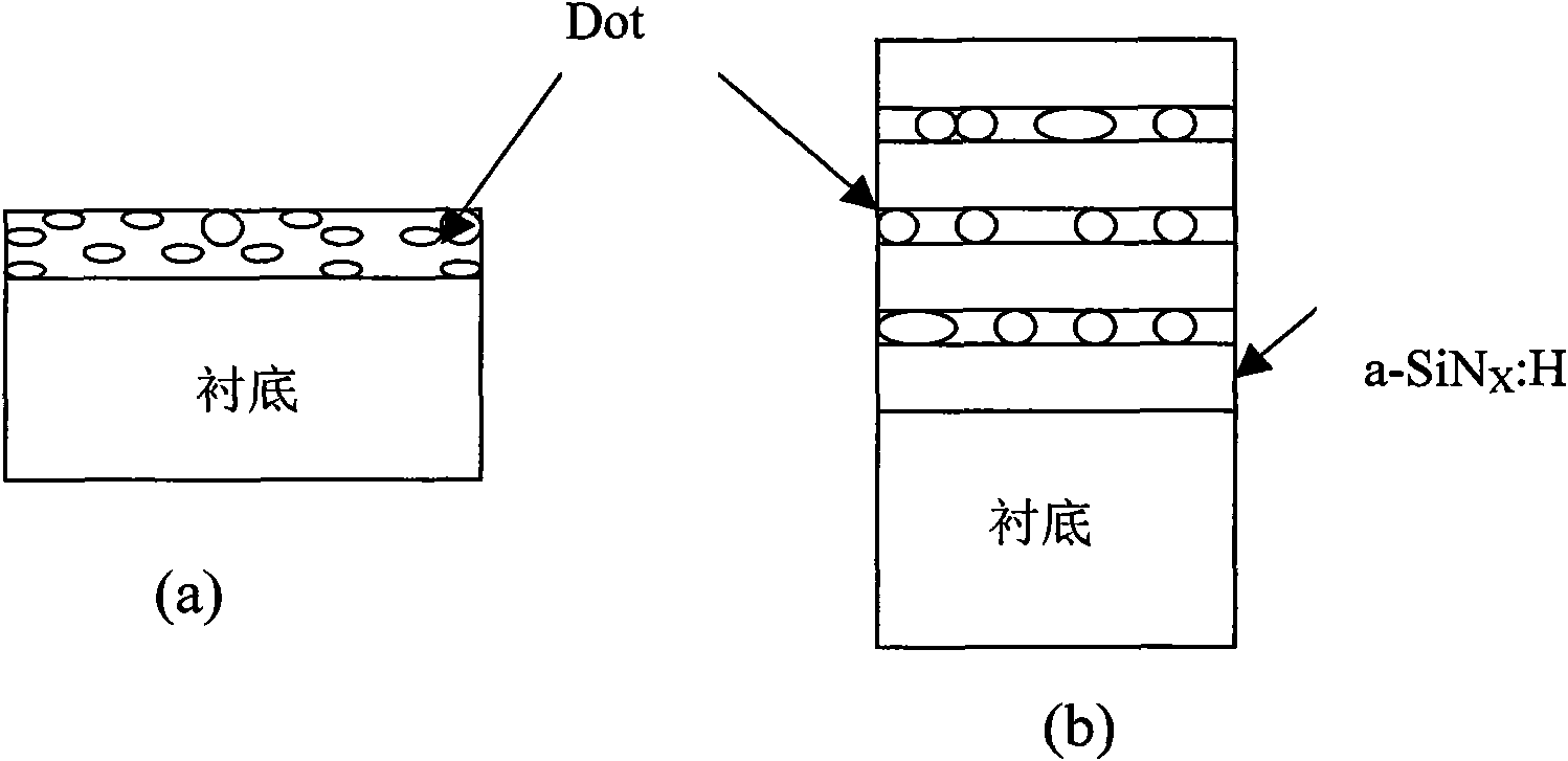
[0029] (1) Preparation of ultra-thin doped amorphous silicon monolayer film

[0030] A flat capacitive RF plasma-enhanced chemical vapor deposition (PECVD) device was used as the growth system, and the reaction gas source was silane (SiH) with a volume mixing ratio of 5:1-10. 4 ) and phosphine (PH 3 ) (or use B 2 h 6 Prepare B-doped amorphous silicon film) mixed gas, select a lower ratio for light doping, and choose a higher ratio for heavy doping. The substrate is made of single crystal silicon wafer, qua...

Embodiment 2

[0039] The method for realizing the controllable doping of nano-silicon quantum dots in this embodiment combines the doped amorphous silicon multilayer film with laser crystallization technology, and uses appropriate energy laser to induce the crystallization of the doped amorphous silicon layer in the multilayer film to obtain Nano silicon quantum dot multilayer film with controllable doping concentration. Specific steps are as follows

[0040] 1. Preparation of basic materials:

[0041] (1) Preparation of confinement layer

[0042] The substrate material is placed on the grounded metal plate in the reaction chamber of the radio frequency plasma enhanced chemical vapor deposition equipment, and the gas source is silane (SiH 4 ) and ammonia (NH 3 ) mixed gas with a mixing ratio of 5:1-10, start the RF switch, deposit a 10-100nm thick hydrogenated amorphous silicon nitride (a-SiNx:H) film on the substrate material, and turn off the RF switch after completion ;

[0043] (2)...


PUM

PropertyMeasurementUnit
Wavelengthaaaaaaaaaa
Power densityaaaaaaaaaa

Abstract

The invention relates to a method for realizing controlled doping of nano silicon quantum dots, which belongs to the technical field of nano photoelectronic devices. The method comprises the steps of preparing a doped amorphous silicon film, preparing a doped amorphous silicon multilayer film, preparing doped nano silicon quantum dots in virtue of laser radiation, and the like. The invention provides a preparation method for convenient, rapid and effective controlled doping of the nano silicon quantum dots, and the method has short processing time, does not damage a film and a substrate in a nanosecond level, and is compatible with the current micro-electronics processing technology. In the implementation process, the method mainly adopts a high-energy laser to irradiate the surface of the film to obtain the nano silicon quantum dots with uniform size, simultaneously realize the controlled doping of impurity concentration and improve the photoelectric property of the film. The doped nano silicon quantum dots prepared by the method have wide application prospect in the fields of future nanoelectronics, nano photoelectronic devices and the like.

Description

technical field [0001] The invention relates to a method for doping nano-silicon quantum dots, in particular to a method for realizing controllable doping of nano-silicon quantum dots, which belongs to the technical field of nano-optoelectronic devices. Background technique [0002] In the research process of semiconductor materials and devices, amorphous silicon thin film, as a photoelectric material, has become the focus and core of amorphous semiconductor material research, and is widely used in various devices, such as thin film transistors (TFT) and thin film solar cells Wait. Due to the continuous improvement of the efficiency of thin-film solar cells and the continuous improvement of device performance, people's requirements for materials are also constantly updated. However, due to some shortcomings of the amorphous silicon material itself, such as low electrical conductivity and poor light stability, the amorphous silicon material is limited. Further applications o...

Claims


Application Information

Patent Timeline
IPC IPC(8): B82B3/00
Inventor 徐骏宋超陈谷然黄信凡李伟陈坤基马忠元徐岭
Owner NANJING UNIV
Why Eureka
Try Eureka