Preparation methods of ZnO base powder target and thin film transistor active layer

A thin-film transistor and powder target technology, which is applied in coating, metal material coating process, ion implantation plating, etc., can solve problems such as easy cracking during use, complex target manufacturing process, and easy introduction of impurities, etc., to achieve optimization The device structure and deposition conditions of each layer, the effect of performance index improvement and cost reduction

Inactive Publication Date: 2010-06-23
INESA ELECTRON
View PDF1 Cites 11 Cited by
  • Summary
  • Abstract
  • Description
  • Claims
  • Application Information

AI Technical Summary

Problems solved by technology

[0005] The object of the present invention is to provide a kind of powder target and its preparation method, and the preparation method of ZnO-based thin film transistor active layer, described this powder target and its preparation method, and the preparation method of ZnO-based thin film transistor act

Method used


Image

  • Preparation methods of ZnO base powder target and thin film transistor active layer
  • Preparation methods of ZnO base powder target and thin film transistor active layer
  • Preparation methods of ZnO base powder target and thin film transistor active layer

Examples


Embodiment 1

[0039] This example is about the detailed process of ZnO-based powder target preparation and TFT device manufacturing.

[0040] 1. Preparation of powder target

[0041] 1) Preparation of mixed powder

[0042] Put the required ZnO powder (purity 4N), or doped Ga 2 o 3 、In 2 o 3 (Purity is 5N) ZnO powder (Ga 2 o 3 : In 2 o 3 : ZnO molar ratio is 0.5: 0.5: 1.0), put it into a cleaned ball mill jar, and put an agate ball with a diameter of about 1 cm, using analytical pure ethanol as the medium, the mass ratio of ball: material: medium is about 2: 1 : 1, ball milled on a roller ball mill for 5 hours, then poured the mixed slurry into a glass beaker and dried at 180-200°C.

[0043] 2) Powder filling seat and pressure head production

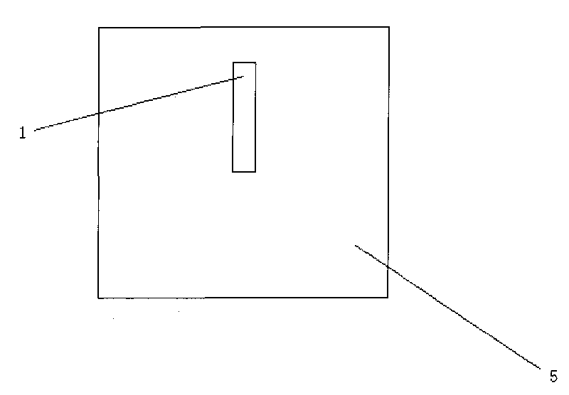
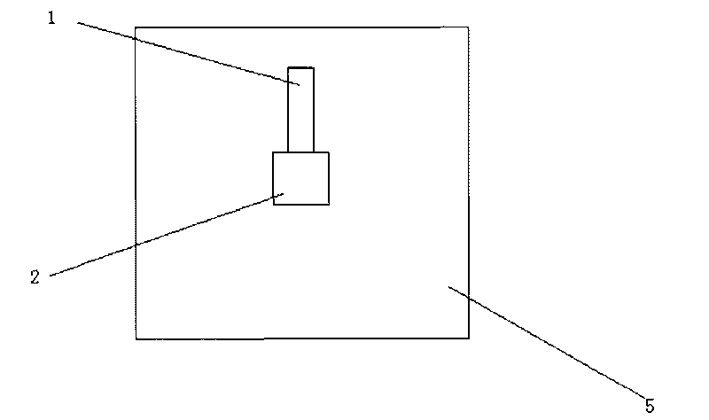
[0044] Process the aluminum alloy packing groove (the material is provided by Shanghai Lizhi Materials Co., Ltd., model 7009), an aluminum alloy disc with a thickness of 7mm and a diameter of 7.6cm, and a concentric groove is milled in the m...

Embodiment 2

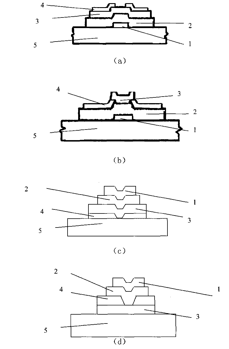
[0059] For a top-gate TFT device with IGZO as the active layer, the ratio of width (W) / length (L) of the device channel is 200 μm / 25 μm. The pattern of each layer is obtained by using a SUS430 stainless steel mask plate with a thickness of 50 μm. In order to reduce the gap between the mask and the substrate, a strong magnet of the same size is placed on the back of the substrate. Glass substrate using CorningEagle 2000, size 35×35mm 2 , after cleaning according to standard steps (see: Chinese patent, application number: 200810032549.3). The source-drain Ni electrode with a thickness of 40nm is evaporated by electron beam, and the deposition equipment is ZZSX-800 electron beam coating machine, and the vacuum degree of the chamber during deposition is 3.5×10 -3 Pa. Then, a 40nm IGZO thin film was deposited as an active layer using a powder target, and the deposition equipment was a CS500 radio frequency magnetron sputtering apparatus. The diameter of the target is 3 inches, a...

Embodiment 3

[0066] For a top-gate TFT device with IGZO as the active layer, the ratio of width (W) / length (L) of the device channel is 200 μm / 50 μm. The test of glass substrate and cleaning method, source-drain electrode, active layer, gate dielectric, gate electrode material and deposition method, thickness and electrical performance characteristics are all the same as in Example 2 except for the differences described below . The thickness of the IGZO active layer is 50nm, and the background vacuum during deposition is 7.4×10 -4 Pa, Ar / M (M stands for Ar and O 2 mixed gas, O 2 The content is 4.7%), the flow ratio is 120sccm / 5sccm, the air pressure is 1.4Pa, the power is 150W, the substrate temperature is about 20°C, the target-base distance is 6.4cm, and the deposition rate is 9.8nm / min. Gate dielectric uses Al 2 o 3 (70nm) / sialon (400nm) composite structure, the deposition power of sialon is 400W, the deposition rate is 10.9nm / min, and the rest are the same as in Example 2. al 2 ...


PUM

PropertyMeasurementUnit
Thicknessaaaaaaaaaa
Electrical breakdown strengthaaaaaaaaaa
Field effect mobilityaaaaaaaaaa

Abstract

The invention discloses a powder target which comprises ZnO or multiple metal oxide powders of InwGaxSnyZnzOu mainly comprising the ZnO. The invention also discloses a preparation method of the powder target and also discloses a preparation method of a thin film transistor active layer. The preparation method of the thin film transistor active layer comprises the steps of: preparing the powder target, wherein the powder target comprises the ZnO or multiple metal oxides mainly comprising the ZnO; arranging a filling groove on a high heat conduction metal base, arranging a powder block body which is tightly combined with the filling groove and has high compactness in the filling groove; and then depositing the thin film transistor active layer by adopting a radio frequency magnetron sputter plating method. The preparation method of the ZnO base powder target has simple operation and low use and maintenance cost. The high-quality thin film transistor active layer is deposited to be used as a sputtering target, and the prepared thin film transistor has excellent performance.

Description

Technical field: [0001] The invention belongs to the field of semiconductor devices, and in particular relates to a powder target, a preparation method thereof, and a preparation method of an active layer of a ZnO-based thin film transistor. Background technique: [0002] ZnO-based TFT is considered to be the next-generation MOSFET that is most likely to replace the current large-scale industrialized a-Si:H TFT, and has attracted widespread attention in recent years. The mature a-Si:H TFT has gradually revealed its limitations, mainly low mobility and opacity, so the response speed and aperture ratio of the device are limited. The second outstanding problem of a-Si:H TFT is the small band gap (1.7eV), which requires a black matrix to block visible light irradiation, so as not to generate additional photogenerated carriers, which increases the complexity and cost of the process. If the black matrix is ​​not used, only the structure of the bottom gate can be used. The third ...

Claims


Application Information

Patent Timeline
IPC IPC(8): C23C14/08C23C14/35
Inventor 林明通肖田陈科张羿
Owner INESA ELECTRON
Why Eureka
Try Eureka