Vanadium oxide thin film for microbolometer and preparation method thereof

A microbolometer, vanadium oxide thin film technology, applied in electrical radiation detectors, resistor manufacturing, superimposed layer plating, etc. The preparation process is difficult and other problems, to achieve the effect of being suitable for large-scale industrial production, improving poor chemical stability, and excellent chemical stability

Inactive Publication Date: 2010-12-15
UNIV OF ELECTRONIC SCI & TECH OF CHINA
View PDF4 Cites 11 Cited by
  • Summary
  • Abstract
  • Description
  • Claims
  • Application Information

AI Technical Summary

Problems solved by technology

However, since the electronic structure of the vanadium atom is 3d 3 4s 2 , the 4s and 3d orbitals can lose part or all of their electrons. Therefore, the traditional preparation methods of vanadium oxide films, such as magnetron sputtering, electron beam evaporation, laser pulse deposition, etc., have their own insurmountable shortcomings: namely The valence state of the V element in the prepared vanadium oxide thin film is complex, and the stability of the chemical structure of the thin film is poor, etc.
Due to the complex composition of the V element, small changes in the preparation process will have a greater impact on the chemical composition of the vanadium oxide film, resulting in significant changes in the electrical and optical properties of the film, which in turn affect the performance of the device.
Therefore, one of the main disadvantages of the microbolometer based on vanadium oxide film is that the preparation process of vanadium oxide film is difficult, and the repeatability and stability of the product are poor.
The disadvantage of co-sputtering metal doping is that the sputtering rate of metal impurities and vanadium oxide is difficult to keep consistent, so the ratio of vanadium oxide to metal in the

Method used


Image

  • Vanadium oxide thin film for microbolometer and preparation method thereof
  • Vanadium oxide thin film for microbolometer and preparation method thereof
  • Vanadium oxide thin film for microbolometer and preparation method thereof

Examples


Example Embodiment

[0028] The present invention will be further described below in conjunction with the drawings:

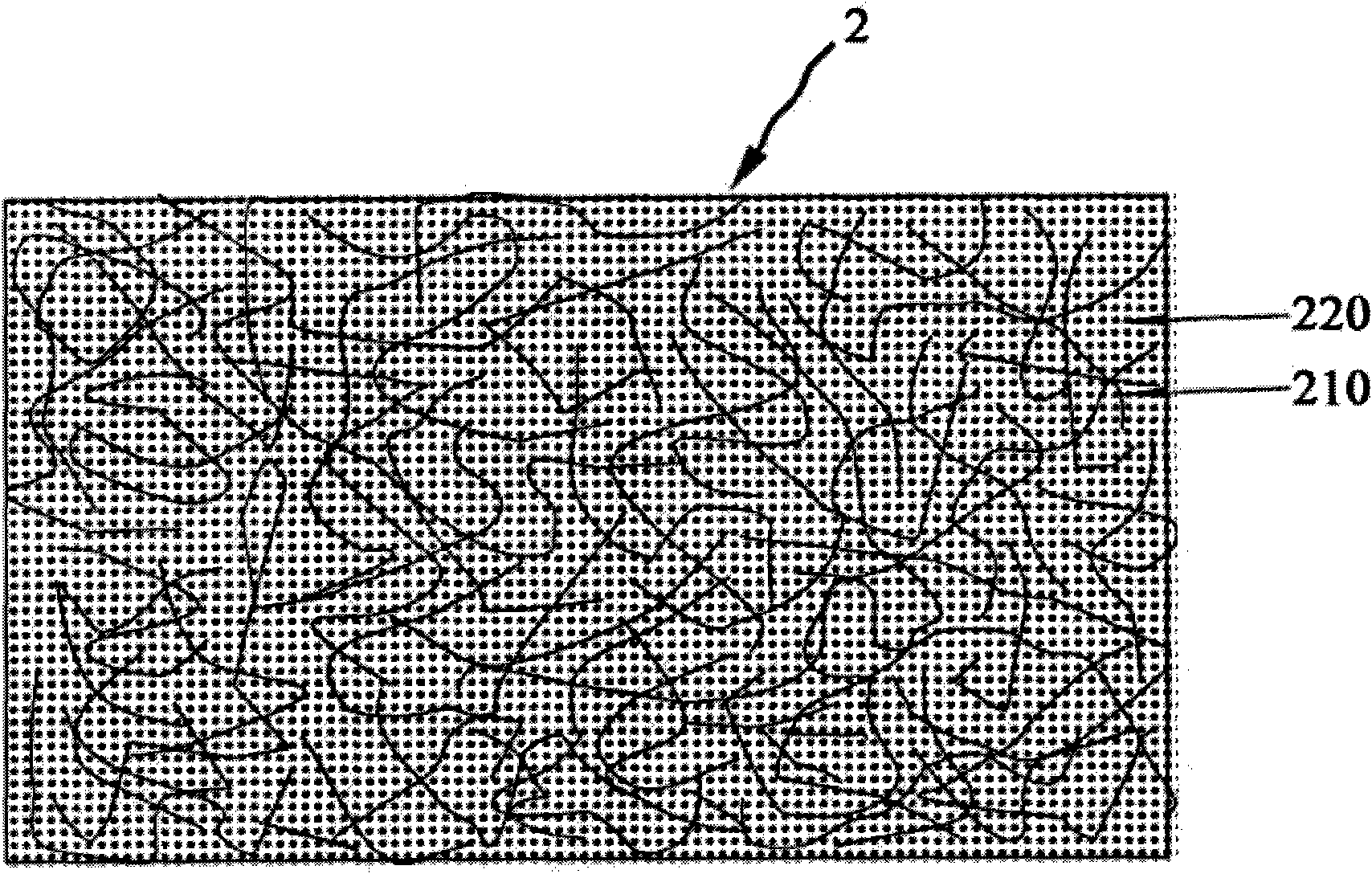
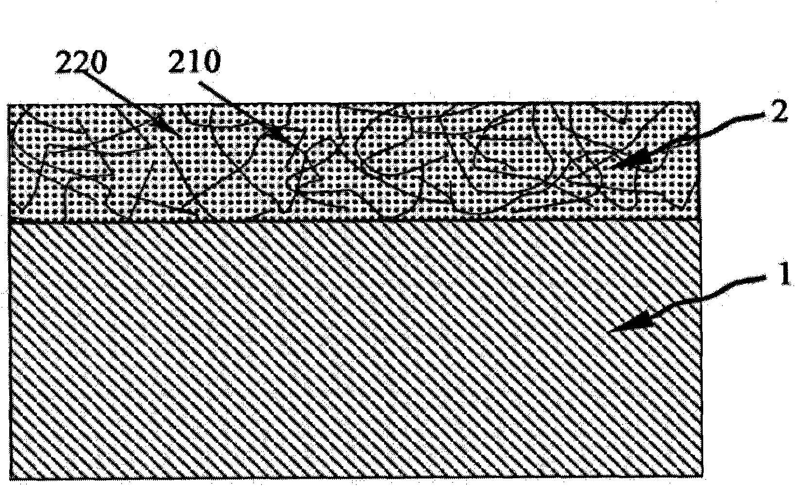
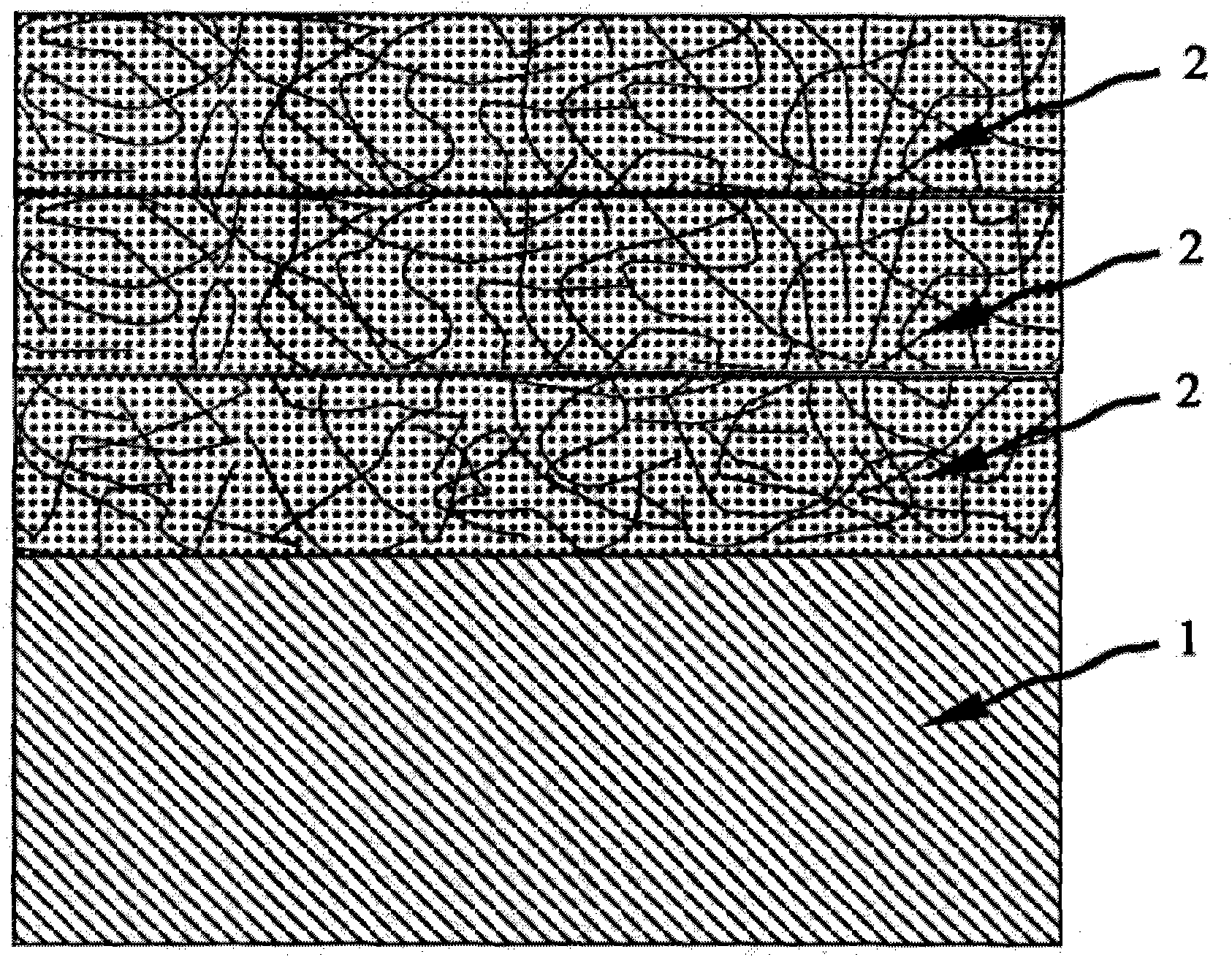
[0029] The guiding ideology of the present invention is to use the excellent electrical and optical properties of carbon nanotubes and vanadium oxide in the vanadium oxide-carbon nanotube composite film structure to prepare a composite film with relatively good comprehensive performance (such as figure 1 (Shown), used as the thermistor material and light absorbing material of the uncooled microbolometer to improve the performance of infrared detectors or terahertz detectors. The embodiment of the present invention for preparing the vanadium oxide-carbon nanotube composite film is as follows: ① A silicon wafer with a silicon dioxide film grown on the surface is selected as the substrate 1 for film growth, first ultrasonic cleaning with acetone, and then ultrasonic cleaning with methanol Bottom 1, and then dry it with nitrogen; ② Put the clean substrate 1 into a vacuumized reactor, firs...


PUM


Abstract

The invention discloses a method for preparing a vanadium oxide thin film for a microbolometer. The method is characterized by comprising the following steps of: (1) cleaning and blow-drying a substrate for later use; (2) performing reaction directly on the surface of the cleaned substrate to grow a net-like or intersected and interconnected carbon nano-tube film by using one of a chemical vapor deposition system reactor, an arc discharge system reactor and a laser ablation deposition system reactor and through the induction of a metal catalyst; (3) placing the substrate where the carbon nano-tube film grows into a vacuumized reactor, growing a layer of vanadium oxide film by using the reactor, dispersing the grown vanadium oxide film on the surface of carbon nano-tubes and in the gaps among the tubes, and annealing to form a vanadium oxide-carbon nano-tube composite film structure; (4) cooling the structure to room temperature and taking the structure out of the reactor; and (5) according to requirements, repeating the steps of carbon nano-tube growth, vanadium oxide deposition and annealing sequentially to form a vanadium oxide-carbon nano-tube multi-layer composite film structure.

Description

technical field [0001] The invention relates to the technical fields of uncooled infrared detection and uncooled terahertz detection, in particular to a thermistor material and light-absorbing material of a microbolometer, and a preparation method thereof. Background technique [0002] Infrared detectors convert invisible infrared heat radiation into detectable electrical signals to realize the observation of external affairs. Infrared detectors are divided into two categories: quantum detectors and thermal detectors. Thermal detectors, also known as uncooled infrared detectors, can work at room temperature, have the advantages of good stability, high integration, and low price, and have broad application prospects in military, commercial, and civilian fields. Uncooled infrared detectors mainly include three types: pyroelectric, thermocouple, and thermistor. Among them, the microbolometer focal plane detector based on thermistor is a kind of uncooled infrared detector that ...

Claims


Application Information

Patent Timeline
IPC IPC(8): G01J5/20C23C28/04H01C7/00H01C17/075
Inventor 许向东蒋亚东杨书兵
Owner UNIV OF ELECTRONIC SCI & TECH OF CHINA
Why Eureka
Try Eureka