Microfluidic chip and manufacturing method thereof

A microfluidic chip and microfluidic technology, applied in chemical instruments and methods, instruments, laboratory utensils, etc., can solve problems such as complex structure, passive valve cannot be actively opened, closed or switched, and complex preparation process.

Inactive Publication Date: 2011-05-18
INST OF CHEM CHINESE ACAD OF SCI
View PDF0 Cites 66 Cited by
  • Summary
  • Abstract
  • Description
  • Claims
  • Application Information

AI Technical Summary

Problems solved by technology

According to whether the microvalve has a power drive mechanism, it is divided into active valve and passive valve. The valve can realize the opening and closing of the valve, the braking performance is good, and the airtightness is high, but the disadvantage is that the structure is complex, the volume is large, and it is difficult to realize the integration on the microfluidic chip.
The passive valve does not require external dynamic braking, and relies on the pressure difference on both sides of the valve to realize the switch of the valve, and the volume is small, but the passive valve cannot actively open, close or switch the valve.
A

Method used


Image

  • Microfluidic chip and manufacturing method thereof
  • Microfluidic chip and manufacturing method thereof

Examples


preparation example Construction

[0050] According to the present invention, the preparation method of the microfluidic chip comprises:

[0051] (1) bonding the upper chip unit and the lower chip unit to each other, the surface of the upper chip unit and / or the lower chip unit includes a liquid storage hole, a fluid channel communicated with the liquid storage hole and a micro channel communicated with the fluid channel, The surface of the microchannel is formed with an arrayed three-dimensional micron and three-dimensional nanoscale structure, an arrayed three-dimensional microstructure, or an arrayed three-dimensional nanostructure, and the bonding method makes the microchannel closed on the upper chip Between the unit and the lower chip unit;

[0052] The preparation method of the upper chip unit and / or the lower chip unit includes forming a liquid storage hole, a fluid channel and a microchannel on the surface of the substrate of the upper chip unit and / or the lower chip unit, so that the liquid storage ho...

Embodiment 1

[0066] This example is used to illustrate the preparation of microfluidic chip

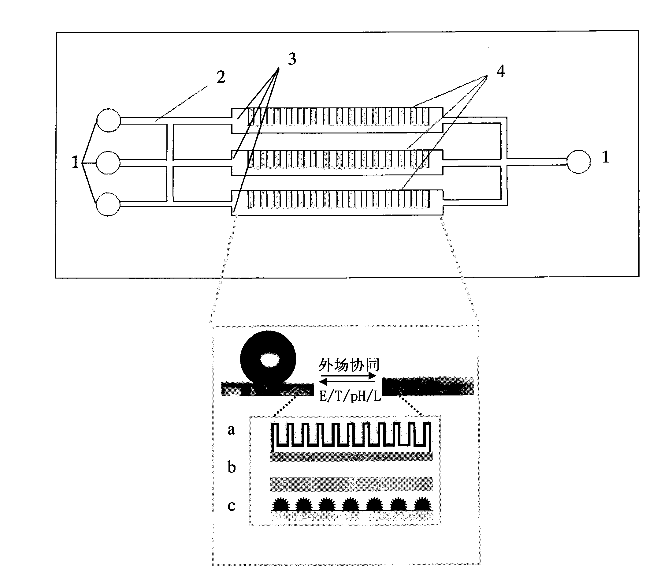
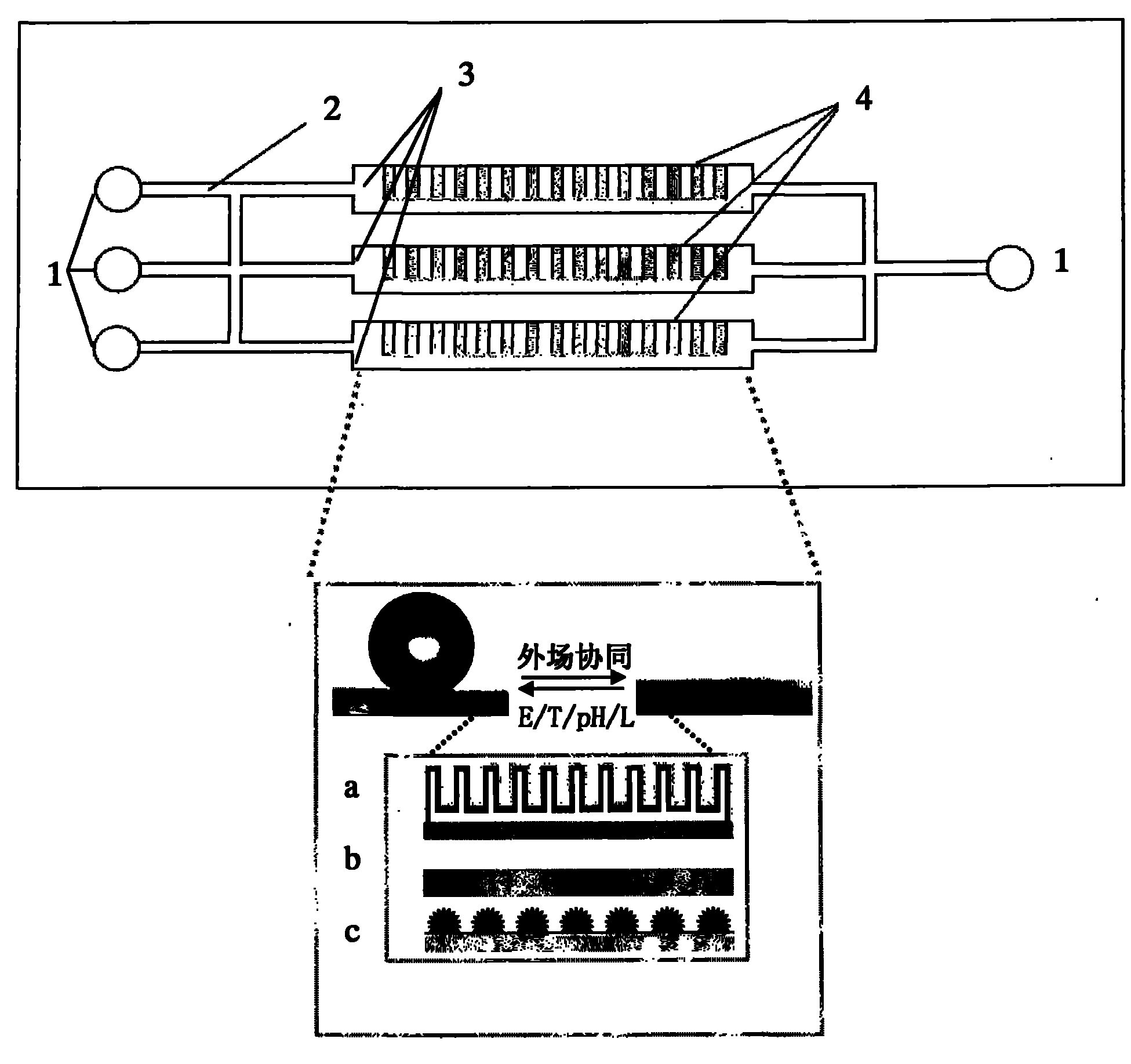
[0067] Such as figure 1 As shown, the design graph of the microfluidic chip is drawn by computer-aided design (CAD), and according to the design drawing, laser etching is used to engrave the surface of a quartz plate (4 cm in length, 3 cm in width, and 1 mm in thickness). Etch out the required chip reservoir hole 1 (round hole with a diameter of 1 mm), fluid channel 2 (20×0.3×0.3 mm (length / width / depth)) and microchannel 3 (15×0.2×0.2 mm ( length / width / depth)). Wash the quartz plate successively with deionized water, ethanol, acetone, and deionized water, and dry it at 100°C.

[0068] Zinc oxide (ZnO) nanowire arrays are prepared on the surface of microchannels by a two-step solution method: ZnO sol is evenly coated on the quartz surface with microchannels, and annealed at 420 ° C to form a layer of 100-200 nm thick seed crystals The membrane was then immersed in an aqueous solution of zinc nit...

Embodiment 2

[0072] This example is used to illustrate the preparation of microfluidic chip

[0073] Such as figure 1As shown, the design graphics of the microfluidic chip are drawn by computer-aided design (CAD). According to the design drawing, an excimer laser etching machine is used to carve the surface of a piece of quartz (5 cm in length, 4 cm in width, and 2 mm in thickness). Etch out the required chip reservoir holes (circular holes with a diameter of 2 mm), fluid channels (20×0.2×0.2 mm (length / width / depth)) and microchannels (15×0.2×0.2 mm (length / width / depth)), clean the substrate surface with deionized water, ethanol, deionized water, ethanol, and let it dry naturally.

[0074] Through a two-step method: soft etching and chemical etching, papillary cone array micro and nano hierarchical structures are prepared in the microchannel, the simple steps are as follows: use a photomask prepared by a chromium layer, expose it through a photolithography machine, Transfer the pattern ...


PUM

PropertyMeasurementUnit
The average diameteraaaaaaaaaa
Lengthaaaaaaaaaa
Widthaaaaaaaaaa

Abstract

The invention relates to a microfluidic chip and a manufacturing method thereof. The microfluidic chip comprises an upper chip unit and a lower chip unit; the surfaces of the chip units are respectively provided with a liquid storing hole, a liquid channel communicated with the liquid storing holes and a microchannel communicated with the liquid channel; the upper chip unit and the lower chip unit are attached to each other and the microchannel is sealed between the two chip units; the microfluidic chip also comprises a micro valve, wherein the micro-valve main body is one of the following structures: a three-dimensional micrometer and three-dimensional nanometer hierarchical structure of polymers formed on the microchannel in array arrangement, a three-dimensional micrometer structure ofpolymers formed on the microchannel in array arrangement or a three-dimensional nanometer structure of polymers formed on the microchannel in array arrangement; the polymers can generate specific responses to an external field under the action of the external field; and the specific responses are reversibility transformation of one or more of surface chemical compositions of the polymers, the above structures and surface properties, thus realizing controllable operations for the flow state of a microfluid in the microchannel. The micro valve in the microfluidic chip is manufactured in situ and miniaturized on the microfluidic chip, thus realizing switch gradient control for the flow of the microfluid and fast switch reversibility transformation.

Description

technical field [0001] The invention relates to a microfluidic chip and a preparation method thereof. Background technique [0002] In recent years, as a new type of analysis platform, microfluidic chips have the advantages of miniaturization, automation, integration, convenience and speed, and have been widely used in many fields, such as cell biology, analytical chemistry, and environmental monitoring. and protection, forensic identification, drug synthesis and screening, materials science and tissue engineering and other fields. In the microfluidic chip, the precise injection of a small amount of liquid is the key to sample processing and analysis. The characteristic is to operate and control the microfluid at the microscopic scale, and the amount of fluid as the object of operation and control is extremely small, resulting in the flow characteristics of the microfluid being very different from the macroscopic, which can be ignored at the macroscopic scale. It becomes t...

Claims


Application Information

Patent Timeline
IPC IPC(8): B01L3/00B01J19/00G01N35/00
Inventor 聂富强江雷朱道本
Owner INST OF CHEM CHINESE ACAD OF SCI
Why Eureka
Try Eureka