Long-range plasmon waveguide array synergy unit for solar cell

A technology of solar cells and waveguide arrays, applied to electrical components, circuits, light guides, etc., to achieve obvious synergistic effects, increase utilization, and improve absorption efficiency

Active Publication Date: 2011-09-14
SOUTHEAST UNIV
View PDF6 Cites 17 Cited by
  • Summary
  • Abstract
  • Description
  • Claims
  • Application Information

AI Technical Summary

Problems solved by technology

[0004] At present, in the field of solar cell technology, it is not uncommon to use metal nanoparticles to increase the efficiency of solar cells, but the technology of using plasmonic waveguide arrays to improve the efficiency of solar cells has not been reported.

Method used


Image

  • Long-range plasmon waveguide array synergy unit for solar cell
  • Long-range plasmon waveguide array synergy unit for solar cell
  • Long-range plasmon waveguide array synergy unit for solar cell

Examples


Embodiment 1

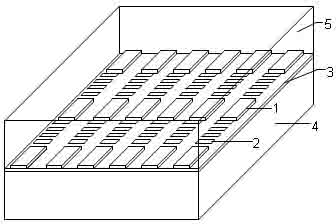
[0024] Example 1: Preparation of a long-range plasmonic waveguide array synergist unit. First, clean and polish the surface of the glass substrate to make the surface flatness at least less than 1 nm, and then use magnetron sputtering deposition, vacuum evaporation deposition, sol- A thin layer of indium tin oxide (ITO) is prepared on a glass substrate by one of the gel method, electrostatic spray-assisted vapor deposition method and high-current pulsed ion beam method, and the flatness is required to be not less than 2nm. The ITO glass is cleaned and dried again, and then a layer of positive photoresist ZPU450 is spin-coated on its surface, and a mask plate matching the metal waveguide array and diffraction grating structure is used for mask exposure. Then develop with a developer, and a photoresist pattern opposite to the structure of the metal waveguide array and the diffraction grating can appear on the surface of the ITO after development. Coating a layer of gold film on ...

Embodiment 2

[0025] Example 2: Preparation of photoanodes for dye-sensitized solar cells Utilize conventional preparation techniques such as sol-gel method, hydrothermal synthesis method, electrophoretic deposition method, magnetron sputtering method, etc. to prepare photoanodes required by the present invention (such as Figure 4 ). Firstly, the transparent conductive film 7 is prepared on the glass substrate 6, and the conductive material of the transparent conductive film is required to be indium tin oxide (ITO) with a thickness of 30-90 nm.

[0026]The semiconductor film is a porous nano film 8, the material is ZnO, and the diameter of the hole is 20-90nm. Then coat a layer of dye sensitizer 9 on the peninsula surface. The dye sensitizer is one of the bipyridine metal complex series, phthalocyanine series, porphyrin series, and pure organic dye series, and the bipyridine metal complex N719 is preferred.

Embodiment 3

[0027] Example 3: Preparation of solar cells Combining the above-mentioned long-range plasmonic waveguide array synergist unit with the photoanode of the dye-sensitized solar cell requires that the side of the photoanode with the dye sensitizer be combined with the side of the synergist unit with the electrolyte , the packaging is firm, and the preparation of the dye solar cell can be completed.


PUM


Abstract

The invention belongs to the technical field of solar cells, in particular to a long-range plasmon waveguide array synergy unit for a solar cell. The specific structure of the long-range plasmon waveguide array synergy unit consists of a long-range plasmon waveguide array, a diffraction grating, a transparent conducting thin film, a glass substrate and a photovoltaic material. The long-range plasma laser waveguide array synergy unit is characterized in that: surface plasmons generated by the waveguide array synergy unit are used for localization to enhance the light field strength on the metal waveguide surface and improve the absorptivity of the solar cell to incident sunlight. Through the technology, the absorptivity of the solar cell to incident sunlight is increased under the condition of not affecting the normal absorption of a photovoltaic material on the top layer to the incident light of a light-facing face, and then the photoelectric conversion efficiency of the solar cell isimproved.

Description

technical field [0001] The invention belongs to the technical field of photovoltaic solar cells, and relates to a long-distance plasmon waveguide array booster unit for solar cells. Background technique [0002] Energy issues are one of the most important issues facing society today. With the gradual depletion of fossil fuel energy, finding new and renewable energy sources has become a hot issue in the field of scientific research. Solar energy is an inexhaustible renewable and clean energy for human beings. It has the greatest potential to become the mainstream energy in the world. Its development and utilization have attracted widespread attention. At present, crystalline silicon solar cell technology is relatively mature, and the total energy conversion efficiency has reached more than 20%. It is currently the most widely used solar cell, but its high price and complicated manufacturing process limit its application. Therefore, improving the photoelectric conversion effi...

Claims


Application Information

Patent Timeline
Patent Type & Authority Applications(China)
IPC IPC(8): H01L31/052H01L31/04G02B6/122H01G9/004H01G9/04H01G9/20H01L31/054
CPCY02E10/50
Inventor 张彤朱圣清张晓阳
Owner SOUTHEAST UNIV
Why Eureka
Try Eureka