
Pulse signal generation device

A technology for generating devices and pulse signals, which is applied in the directions of making antennas work in different bands at the same time, mid-position power feeding between antenna endpoints, and structural forms of radiation elements, etc., which can solve unfavorable UWB communication applications, unfavorable device integration, Disadvantages of power consumption and other issues, to achieve the effect of easy miniaturization, simple design, and simple structure

Active Publication Date: 2011-10-05
NAT INST OF INFORMATION & COMM TECH +1
View PDF8 Cites 10 Cited by
  • Summary
  • Abstract
  • Description
  • Claims
  • Application Information

AI Technical Summary

Problems solved by technology

Furthermore, if the group delay characteristic of each circuit is not flat over a wide band, distortion will occur in the pulse waveform
Therefore, this ultra-wideband circuit design is very difficult compared with the narrow-band circuit design, and all circuits requiring ultra-wideband characteristics will become a high-cost device.
[0014] Moreover, in the invention described in the above-mentioned Non-Patent Document 1, Non-Patent Document 2, or Patent Document 1, since the high-frequency pulse signal generator and the ultra-wideband antenna are connected by the transmission line, the Impedance conversion from impedance (generally 50Ω) to space impedance requires an ultra-wideband antenna. If the reflection coefficient of the antenna is not small enough in ultra-wideband, multiple reflections will occur at the connection of the transmission line.
As antennas with such ultra-wideband characteristics, non-resonant antennas and multi-resonant antennas with tapered structures are used. However, since the tapered portion of the non-resonant antenna with a tapered structure needs to be longer in size compared to the wavelength, it cannot be used. It is not conducive to the integration of the entire device if it does not become large, and it is not ideal to use a multi-resonance system antenna from the viewpoint of group delay characteristics, and its structure tends to become complicated
[0015] Furthermore, as in the inventions described in the above-mentioned Non-Patent Document 1, Non-Patent Document 2, or Patent Document 1, the modulation method of passing / blocking the output of the CW signal oscillation circuit by using a high-speed RF switch, due to unnecessary CW signal The leakage exists in essence, so it is not conducive to the application of UWB communication
In addition, since the CW signal oscillation circuit operates, it is also disadvantageous from the viewpoint of power consumption.
[0016] In addition, the inventions described in Patent Document 2 or Patent Document 3 require circuits such as switches that operate at extremely high speed in order to generate radiated high-frequency signal components, and high speed is also required for the driver of the switch, which tends to complicate the circuit. change

Method used


Image

  • Pulse signal generation device
  • Pulse signal generation device
  • Pulse signal generation device

Examples


Embodiment Construction

[0056] Next, an embodiment of a pulse signal generating device according to the present invention will be described based on the drawings.

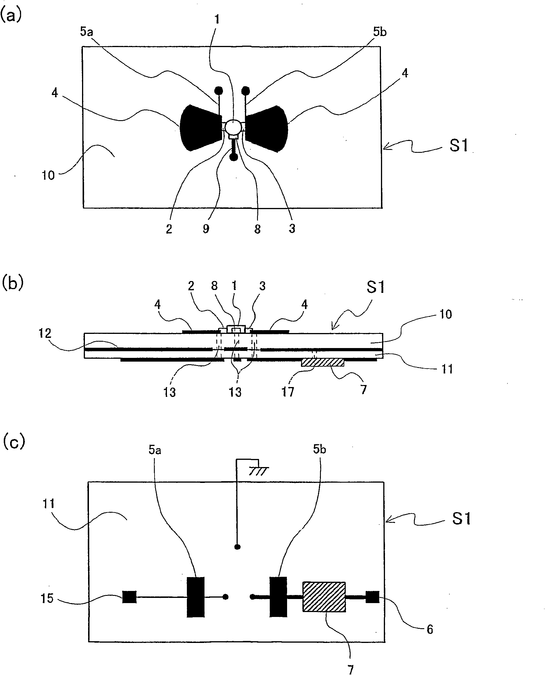
[0057] figure 1 A schematic configuration of a pulse signal generating device (drain-driven high-frequency pulse signal generating device) according to the first embodiment is shown. This pulse signal generating device includes a radiation oscillator substrate S1 and a signal source ( not shown) and a power supply unit (not shown) for DC bias feeding.

[0058] Here, the radiation oscillator substrate S1 functions as a "radiation oscillator that integrates three-electrode high-frequency amplifying elements to generate negative resistance in the resonator, and shares the antenna function of emitting electromagnetic waves in a space". In addition, the three-electrode high-frequency amplifying element is an element that realizes the amplification function by controlling a large current according to a small voltage or current, including a sin...


PUM


Abstract

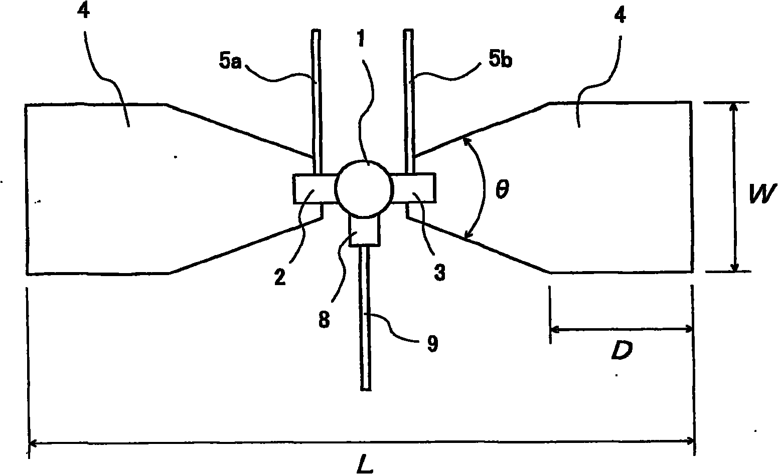
Provided is a microwave-, milliwave-band, high-frequency pulse signal generation device which makes it possible to achieve a simpler structure, improved performance, smaller integration, easier design, lower power consumption, and lower cost. A planar radiation oscillator substrate (S1) having an inner layer (GND12) interposed between a front dielectric substrate (10) and a back dielectric substrate (11) is provided with a pair of axially-symmetrical conductive patches (4, 4) in the radiating surface. A gate electrode (2) and a drain electrode (3) of a microwave transistor (1) are connected to each of the conductive patches (4, 4). A DC bias is supplied through an RF choke circuit (5a) to the gate electrode (2). A monopulse is supplied from a monopulse generation circuit (7) through an RF choke circuit (5b) to the drain electrode (3). An impedance line (9) which satisfies the oscillation conditions is connected to a source electrode (8). A high-frequency pulse signal, having an oscillation frequency and frequency bandwidth which are determined on the basis of the negative resistance generated by the short-time operation of the microwave transistor (1) and a resonant cavity structure, radiates into space simultaneous to being generated.

Description

technical field [0001] The present invention relates to a high-frequency pulse signal generating device for generating an ultra-wideband (UWB: Ultra WideBand) high-frequency pulse signal, and in particular to a device in the microwave / millimeter wave band where complicated circuit configurations are prohibited. High-performance technology. Background technique [0002] As a communication technology attracting attention in recent years, there is UWB technology. Although this technology uses an extremely wide frequency band, the power spectral density is very small, so there is an advantage of being able to share frequencies that are already in use. In addition, by using short pulses of hundreds of picoseconds or less, it is possible to perform high-resolution position detection. [0003] The high-frequency pulse signal generator in the conventional microwave / millimeter-wave band UWB technology is a structure that connects the high-frequency pulse signal generator and the ul...

Claims


Application Information

Patent Timeline
Patent Type & Authority Applications(China)
IPC IPC(8): H01Q23/00H01Q1/38H01Q9/28H03B7/06H04B1/04
CPCH01Q9/285H01Q23/00H01Q19/10H01Q15/0006H01Q13/00H01Q15/0086H01Q5/0017H01Q19/30H01Q5/25
Inventor 歌川仁史松井敏明
Owner NAT INST OF INFORMATION & COMM TECH
Learn More