Groove type atomic gas cavity and atomic clock physical system formed by same

A technology of atomic gas cavity and physical system, which is applied in the field of atomic clock and atomic optics, can solve the problems of low signal-to-noise ratio of CPT signal, short interaction space between laser and alkali metal atomic gas, and reduce the frequency stability of CPT atomic clock, etc., to achieve high The effect of signal-to-noise ratio, CPT atomic clock output frequency signal stability, and low cost

Active Publication Date: 2012-01-18
SHANGHAI INST OF MICROSYSTEM & INFORMATION TECH CHINESE ACAD OF SCI
View PDF5 Cites 36 Cited by
  • Summary
  • Abstract
  • Description
  • Claims
  • Application Information

AI Technical Summary

Problems solved by technology

[0005] The object of the present invention is to provide a trough-type atomic gas chamber and its atomic clock micro-physics system, which is used to solve the problem of the short length of interaction space between laser and alkali metal atomic gas in the optical path of the existing atomic gas chamber structure and its physical system. The signal-to-noise ratio of the CPT signal is low, thereby reducing the frequency stability of the CPT atomic clock

Method used


Image

  • Groove type atomic gas cavity and atomic clock physical system formed by same
  • Groove type atomic gas cavity and atomic clock physical system formed by same
  • Groove type atomic gas cavity and atomic clock physical system formed by same

Examples


Embodiment 1

[0033] Directly bonded and sealed double-layer structure trough-type atomic gas cavity and its constructed atomic clock physical system:

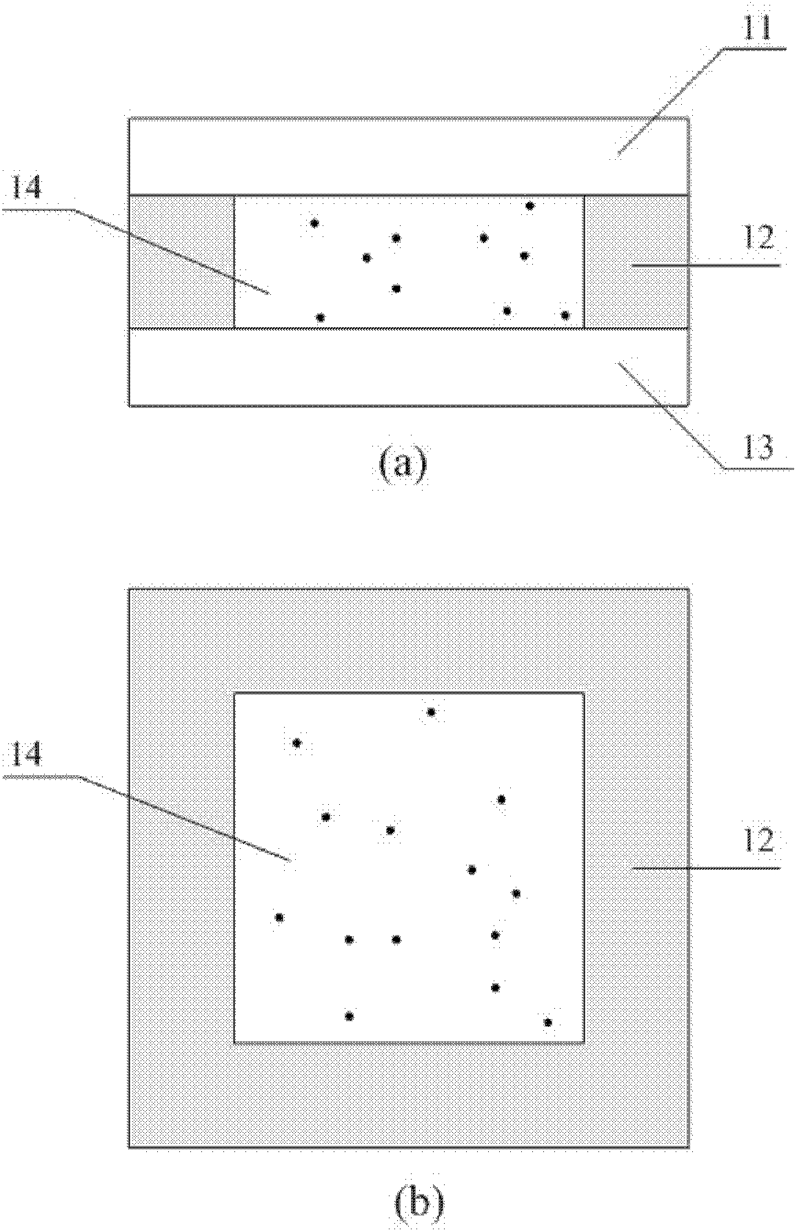
[0034] Figure 4In order to directly bond and seal the double-layer structure groove-type atomic gas cavity, select a silicon wafer with a thickness of 1-3 mm, use silicon dioxide or silicon nitride as a mask, and pass potassium hydroxide or other anisotropic wet The prism-shaped silicon groove structure on the silicon substrate is formed by etching process using the method, and the side wall of the silicon groove structure is the {111} crystal plane. Using evaporation or sputtering technology, using hard mask or lift-off technology, the silicon groove side wall Make a metal film mirror on the surface, and then move the alkali metal element or the compound that reacts to form an alkali metal into the silicon pit in an anaerobic environment, or directly fill it with excess alkali metal vapor, and then fill it with a buffer gas mixed accordi...

Embodiment 2

[0038] The double-layer structure trough-type atomic gas cavity with gas channel sealing and the atomic clock physical system constructed by it:

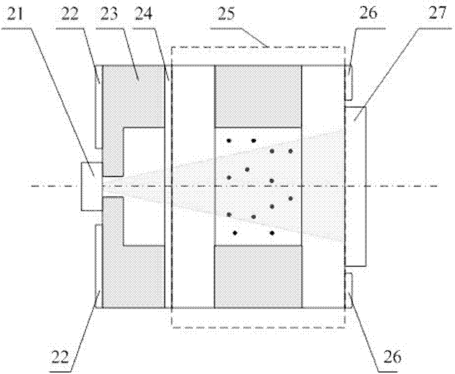
[0039] Figure 5 ~ Figure 7 The double-layer groove-type atomic gas cavity structure is sealed for three kinds of gas channels. The silicon grooves are etched out first in the three structures, and the gas channels are made on the edge of the cavity. The side wall of the silicon groove structure is the {111} crystal plane , use evaporation or sputtering process, use hard mask or lift-off technology, make metal film mirror on the side wall of silicon tank, and then carry out silicon-glass anode bonding, and then pour alkali metal gas and Buffer gas, and finally the cavity is sealed by blocking the gas channel. Figure 5 The form of the gas channel is to make a channel on silicon; Figure 6 The form of the gas channel is to make a channel on the glass, Figure 7 The gas channels in the middle are in the form of through holes on the...

Embodiment 3

[0042] Three-layer structure trough atomic gas cavity and its atomic clock physical system:

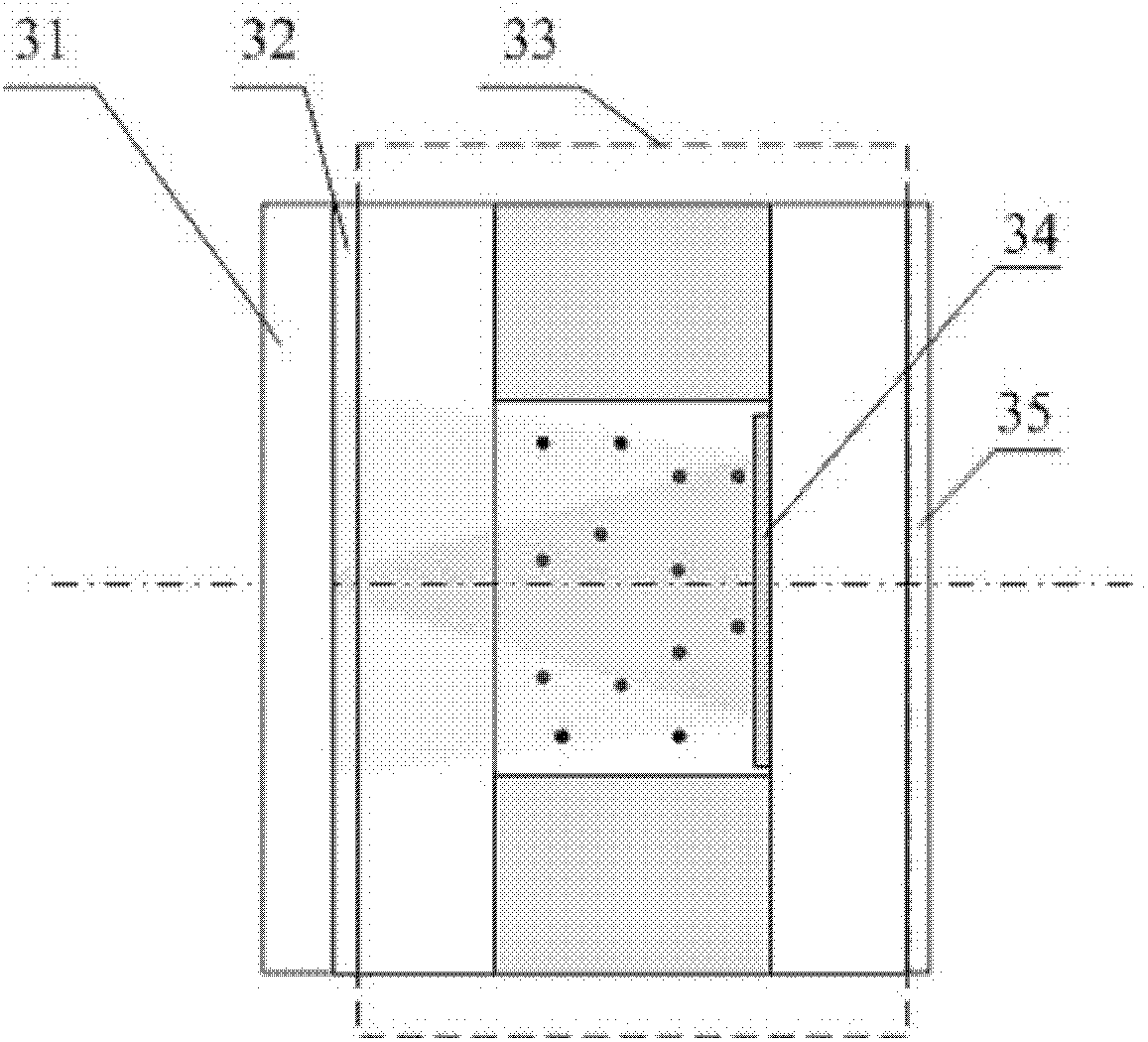
[0043] Similar to the two-layer structure trough-type atomic gas cavity, the three-layer structure trough-type atomic gas cavity also includes a direct bonding sealing structure and a gas channel sealing structure. Figure 8 It is a schematic diagram of the structure of a three-layer groove-type atomic gas cavity with direct bonding and sealing. Select a silicon wafer with a thickness of 1 to 3mm, use silicon dioxide or silicon nitride as a mask, and use potassium hydroxide or other anisotropic wet etching processes to etch the silicon wafer on one side to form a silicon substrate The through-hole structure on the through-hole, the side wall of the through-hole is the {111} crystal plane, and the post-corrosion surface of the silicon wafer is anodically bonded to a piece of Pyrex glass to form a half-cavity structure, using evaporation or sputtering technology, using a hard mask Or ...


PUM


Abstract

The invention relates to a groove type atomic gas cavity produced by applying MEMS technology and an atomic clock physical system formed by the same. The cavity is characterized in that the cavity is formed in such a manner that a silicon wafer with a groove and Pyrex glass sheets define a cavity structure through bonding; the cavity structure is used for alkali metal atom vapor and buffer gases to fill in; the cross section of the groove is in a shape of inverted trapezoid; and the groove comprises a bottom surface and side walls forming included angles with the bottom surface. The cavity is manufactured based on MEMS (micro-electro-mechanical system) technology. The silicon groove is formed through anisotropic etching of the (100) monocrystalline wafer. The groove type cavity is manufactured through silicon-glass anode bonding. The side walls of the cavity are {111} crystal planes of the silicon wafer. The cavity and the system have the following beneficial effects: by utilizing the cavity, the distance between two reflectors in the cavity is easy to enlarge through atomic cavity dimension design, thus increasing the length of the interaction space between laser and atomic gas, enhancing the signal to noise ratio of the CPT (coherent population trapping) signal and being beneficial to improvement of the frequency stability of the micro CPT atomic clock.

Description

technical field [0001] The invention relates to the fields of atomic optics and atomic clocks, in particular to an atomic gas cavity and a micro-physical system of a chip-level CPT atomic clock, which can be used in atomic optical devices and systems such as atomic clocks, atomic magnetometers, and atomic gyroscopes. Background technique [0002] CPT atomic clock is an atomic clock frequency source realized by using two-color coherent light to interact with atoms to prepare atoms into a coherent state, and using CPT signals as microwave frequency discrimination signals. Due to the characteristics of easy miniaturization, low power consumption and high frequency stability, the CPT atomic clock has been valued by research institutions in various countries since it was proposed, and in-depth research has been carried out. Passive CPT atomic clocks do not require microwave resonators and can reduce the size of atomic clocks to the chip level. MEMS technology is used to fabricate...

Claims


Application Information

Patent Timeline
Patent Type & Authority Applications(China)
IPC IPC(8): G04F5/14
Inventor 吴亚明徐静张志强李绍良
Owner SHANGHAI INST OF MICROSYSTEM & INFORMATION TECH CHINESE ACAD OF SCI
Why Eureka
Try Eureka