Solder bump/metallization layer connecting structure body in microelectronic package and application of solder bump/metallization layer connecting structure body

A technology for connecting structural bodies and microelectronic packaging, applied in the field of micro-interconnection, can solve the problems of fatigue failure of connecting bodies, loss of function, consumption of metallization layer, etc. Effect

Active Publication Date: 2012-04-18
INST OF METAL RESEARCH - CHINESE ACAD OF SCI
View PDF5 Cites 4 Cited by
  • Summary
  • Abstract
  • Description
  • Claims
  • Application Information

AI Technical Summary

Problems solved by technology

[0006] In view of the above-mentioned actual situation of the prior art, the purpose of the present invention is to provide a solder bump / metallization (transition) layer connection structure and application thereof in a microelectronic packaging with good solderability, so as to solve the problems existing in the prior art. When the lead-free solder is connected to the metallization layer, it is easy to quickly consume the metallization layer, making it lose its proper function, and the fatigue failure of the connector occurs.

Method used


Image

  • Solder bump/metallization layer connecting structure body in microelectronic package and application of solder bump/metallization layer connecting structure body
  • Solder bump/metallization layer connecting structure body in microelectronic package and application of solder bump/metallization layer connecting structure body
  • Solder bump/metallization layer connecting structure body in microelectronic package and application of solder bump/metallization layer connecting structure body

Examples


Embodiment 1

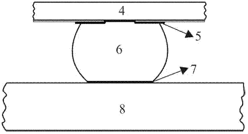
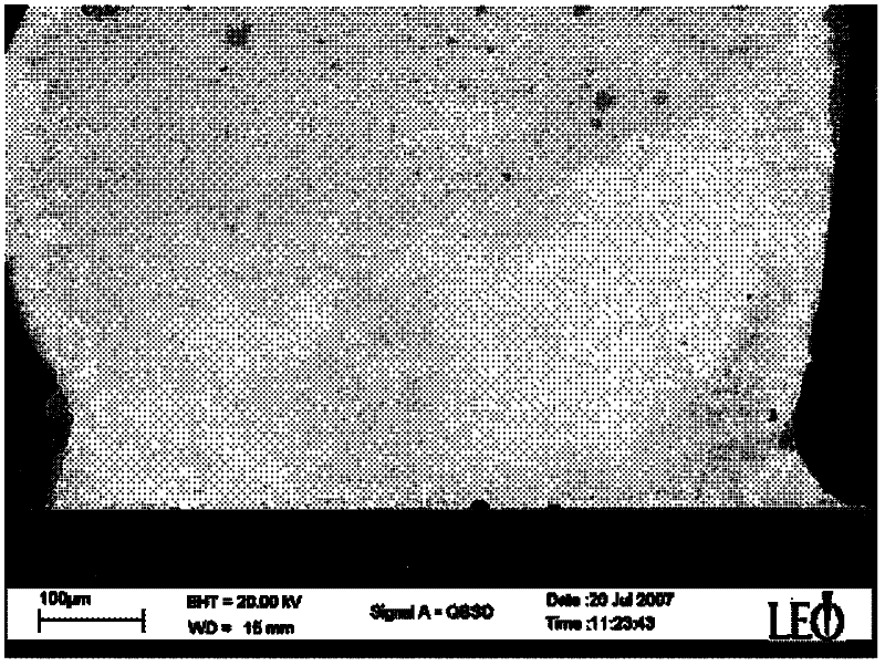
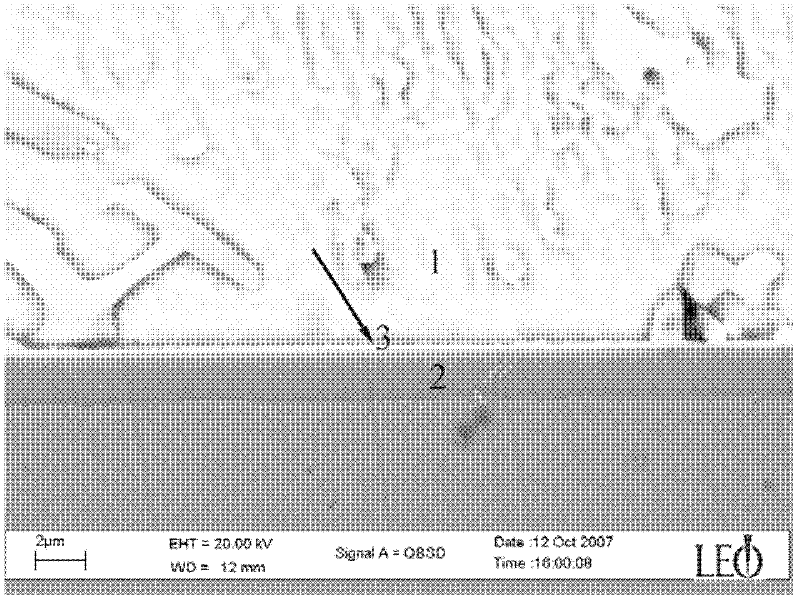
[0040] Electroplate a layer of iron-nickel-cobalt alloy on the surface of a conductive substrate such as copper or nickel, or on the surface of a non-conductive substrate covered by a conductive film. The composition and thickness of the electroplating layer can be adjusted according to actual requirements. Such as figure 1 As shown, the coating realized by the present invention can be used as the iron-nickel-cobalt metallization layer 7 of the pad on the substrate and on the printed circuit board 8, and the lower iron-nickel-cobalt of the tin-silver-copper solder bump 6 in the chip 4 flip-chip welding connection Metallization layer 5 is used. Such as figure 2 As shown, the macroscopic cross-sectional view of the iron-nickel-cobalt plating / tin-silver-copper spherical bump connector.

[0041] A thin layer of iron-nickel-cobalt layer is plated on the copper substrate by means of electroplating, and its composition is: 60% of iron, 35% of nickel and 5% of cobalt (percentage by...

Embodiment 2

[0045] The difference from Example 1 is:

[0046] The composition of the iron-nickel layer is: iron 59%, nickel 35%, cobalt 6%;

[0047] Solder composition: tin 95.8%, silver 3.5%, copper 0.7%.

Embodiment 3

[0049] The difference from Example 1 is:

[0050] The composition of the iron-nickel layer is: iron 63%, nickel 33%, cobalt 4%;

[0051] Solder composition: tin 98.5%, silver 1%, copper 0.5%.


PUM

PropertyMeasurementUnit
thicknessaaaaaaaaaa

Abstract

The invention relates to a micro-interconnection technology in the field of microelectronic package, in particular to a solder bump/metallization (transitional) layer connecting structure body with favorable solderability in the microelectronic package and application of the solder bump/metallization (transitional) layer connecting structure body. The solder bump/metallization (transitional) layer connecting structure body and the application of the solder bump/metallization (transitional) layer connecting structure body are applied to the technical field of manufacturing of bonding pads of substrates and printed circuit boards in general microelectronic connection as well as metallization transitional layers below solder bumps in the flip-chip bonding interconnection. The connecting structure body is formed by connecting the solder bumps with the metallization layer; the metallization layer is an alloy layer formed by co-depositing 59-69 percent by weight of a ferrum element, 31-41 percent by weight of a nickel element and the balance of a cobalt element; and the solder is a tin-silver or tin-silver-copper series lead-free solder alloy with a relatively-high melting point. According to the method, a ferrum-nickel-cobalt alloy layer is plated on a copper (or nickel) layer by adopting an electroplating method. Relative to a ferrum-nickel coating, a small amount of cobalt is added so as to allow the proportion of the contents of the ferrum and the nickel to be maintained at a lower expansion coefficient in a wider range and maintained constant in a wider temperature range.

Description

technical field [0001] The invention relates to the micro-interconnection technology in the field of microelectronic packaging, in particular to a solder bump / metallization (transition) layer connection structure in microelectronic packaging with good solderability and its application, which is suitable for general microelectronic connection The invention relates to the technical field of manufacturing a metallization transition layer on a middle substrate and a printed circuit board pad, as well as under a solder bump in a flip chip interconnection. Background technique [0002] Semiconductor integrated circuit components are called "industrial rice". But in general, what people use is a package with a shell. Electronic packaging has many functions such as mechanical support, electrical connection, external field shielding, stress relaxation, heat dissipation and moisture resistance. Today, the rapid light, thin, short, and miniaturization of electronic equipment promotes...

Claims


Application Information

Patent Timeline
Patent Type & Authority Applications(China)
IPC IPC(8): H01L23/488H01L21/60
CPCH01L2224/16225H01L2924/1461
Inventor 祝清省刘海燕郭敬东尚建库
Owner INST OF METAL RESEARCH - CHINESE ACAD OF SCI
Why Eureka
Try Eureka