Terahertz or infrared micro-bolometer and manufacturing method thereof

A microbolometer and terahertz technology, applied in the field of uncooled terahertz detection, can solve the problems of poor product repeatability and stability, high temperature, and complex valence state of V element in vanadium oxide films.

Inactive Publication Date: 2012-04-25
UNIV OF ELECTRONICS SCI & TECH OF CHINA
View PDF8 Cites 22 Cited by
  • Summary
  • Abstract
  • Description
  • Claims
  • Application Information

AI Technical Summary

Problems solved by technology

However, since the electronic structure of vanadium atom is 3d34s2, the 4s and 3d orbitals can lose some or all electrons, so the traditional vanadium oxide film preparation Methods, such as magnetron sputtering, electron beam evaporation, laser pulse deposition, etc., have their own insurmountable shortcomings: that is, the valence state of the V element in the prepared vanadium oxide film is complex, the stability of the film chemical structure is poor, etc.
Due to the complex composition of the V element, small changes in the preparation process will have a greater impact on the chemical composition of the vanadium oxide film, resulting in significant changes in the electrical, optical and mechanical properties of the film, which in turn affect the performance of the device.
Therefore, one of the main disadvantages of the detector based on vanadium oxide film is: the preparation process of vanadium oxide film is difficult, and the repeatability and stability of the product are poor.
The disadvantages of this inorganic sol-gel method are: (1) the temperature of sol preparation is too high, which affects device integration; (2) the product contains a large amount of non-metallic impurities F, which affects the material properties; (3) the obtained vanadium oxide The light absorption rate is low, which is not conducive to absorption detection
Unfortunately, the traditional organic sol-gel method has some of the same disadvantages as the inorganic sol-gel method, including: (1) The metal impurities in the vanadium oxide film prepared by the organic or inorganic sol-gel method are physically doped, That is, there is no chemical bond between it and vanadium oxide, so this kind of film is prone to impurity diffusion, segregation, etc., resulting in degradation of the performance and quality of the vanadium oxide film, and it is difficult to meet the needs of long-term operation of the device; (2) Metal doping by organic or inorganic sol-gel methods cannot effectively improve the light absorption properties of vanadium oxide films
[0006]On the other hand, the absorption peaks of stretching vibration and bending vibration of various V-O chemical bonds (such as V=O, O-V-O, etc.) of vanadium oxide are in the mid-infrared region (about 10 μm), and in the terahertz range (30~3000 μm), its absorption is weak
Therefore, another major disadvantage of the traditional vanadium oxide film is that it is difficult for this film to meet the optical requirements of terahertz detectors with high sensitivity requirements.
This kind of one-dimensional carbon nanotubes arranged laterally has a disadvantage: that is, the response of one-dimensional carbon nanotubes to light is anisotropic.
[0010]In short, the conductivity, chemical stability, and light absorption performance of vanadium oxide films are insufficient and need to be improved
However, pure carbon nanotubes or pure fullerenes also have some shortcomings in terms of optical or electrical properties, so it is not suitable to use pure carbon nanotubes, pure fullerenes, or ordinary carbon nanotubes. - Polymer composite films, etc. are used as infrared or terahertz light-absorbing materials and thermistor materials, and are directly applied in uncooled infrared detectors or uncooled terahertz detectors

Method used


Image

  • Terahertz or infrared micro-bolometer and manufacturing method thereof
  • Terahertz or infrared micro-bolometer and manufacturing method thereof
  • Terahertz or infrared micro-bolometer and manufacturing method thereof

Examples


Embodiment Construction

[0060] Below in conjunction with accompanying drawing and embodiment the present invention will be further described:

[0061] I. Fabrication of Terahertz or Infrared Microbolometer Based on Vanadium Oxide-Fuller Binary Composite Thin Film

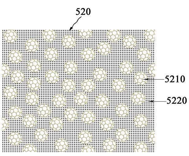
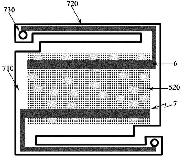
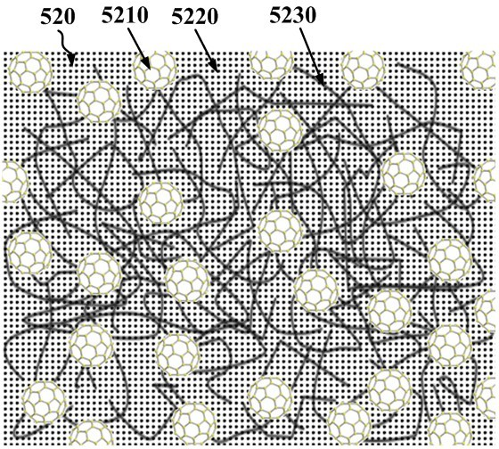
[0062] Using the vanadium oxide-Fuller binary composite film provided by the present invention as the thermistor and light-absorbing material of the terahertz or infrared microbolometer can better control the electrical and optical properties of the material and avoid microbridge sensitivity. Changes in material properties caused by changes in the chemical structure of materials can improve the overall performance of devices. The embodiment of the terahertz or infrared microbolometer based on the vanadium oxide-Fuller binary composite thin film of the present invention is as follows: ① select a silicon wafer containing an integrated circuit (ROIC) as the substrate 1, and use nitrogen gas after cleaning After drying, put it into the plasma...


PUM

PropertyMeasurementUnit
thicknessaaaaaaaaaa
thicknessaaaaaaaaaa
thicknessaaaaaaaaaa

Abstract

The invention discloses a terahertz or infrared micro-bolometer, which comprises a micro-bridge structure of a micro-bolometer for an uncooled terahertz detector or an uncooled infrared detector, wherein a thermistor material and a light absorbing material in the micro-bridge structure are one of a vanadium oxide-fullerene binary composite thin film or a vanadium oxide-fullerene-carbon nanotube ternary composite thin film. The vanadium oxide composite film is formed by compounding two-dimensional vanadium oxide and zero-dimension fullerene components or two-dimensional vanadium oxide, zero-dimension fullerene and one-dimensional carbon nanotube components. The micro-bolometer and a manufacturing method thereof can overcome the defects existing in the prior art and are suitable for large-scale industrial production; and the working performance of the device is improved.

Description

technical field [0001] The invention relates to the technical fields of uncooled terahertz detection and uncooled infrared detection, in particular to a microbolometer and a preparation method thereof. Background technique [0002] Infrared detectors convert invisible infrared heat radiation into detectable electrical signals to realize the observation of external affairs. Infrared detectors are divided into two categories: quantum detectors and thermal detectors. Thermal detectors, also known as uncooled infrared detectors, can work at room temperature, have the advantages of good stability, high integration, and low price, and have broad application prospects in military, commercial, and civilian fields. Uncooled infrared detectors mainly include three types: pyroelectric, thermocouple, and thermistor. Among them, the microbolometer focal plane detector based on thermistor is a kind of uncooled infrared detector that has developed very rapidly in recent years. detectors ...

Claims


Application Information

Patent Timeline
Patent Type & Authority Applications(China)
IPC IPC(8): G01J5/20B81C1/00B32B9/00
Inventor 许向东杨卓蒋亚东何琼敖天宏樊泰君黄龙温粤江
Owner UNIV OF ELECTRONICS SCI & TECH OF CHINA
Why Eureka
Try Eureka