

Preparation method of high-speed low-power-consumption phase change memory
A technology of phase-change memory and phase-change materials, which is applied in the field of microelectronics technology, can solve the problems of reducing operating current, reducing the size of phase-change units, and not having good consistency, so as to achieve high flexibility, low operating current, and fast effect
- Summary
- Abstract
- Description
- Claims
- Application Information
AI Technical Summary
Problems solved by technology
Method used
Image

Examples
example 1
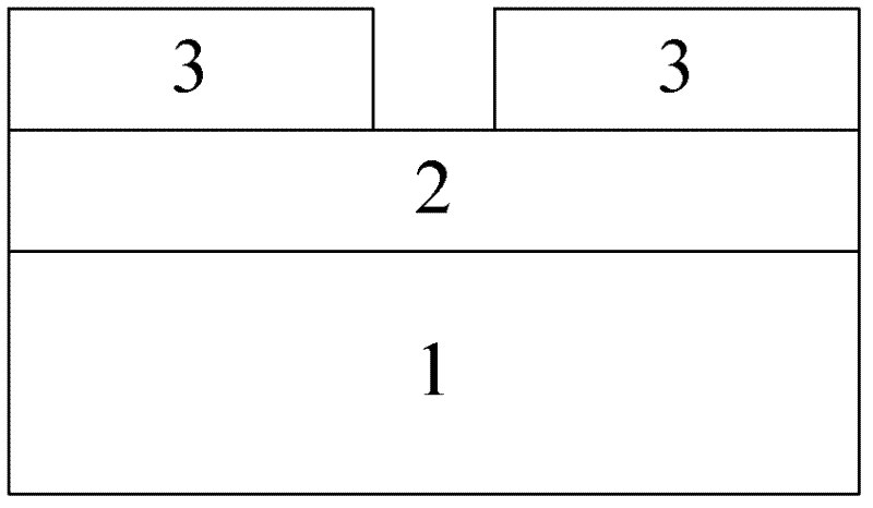
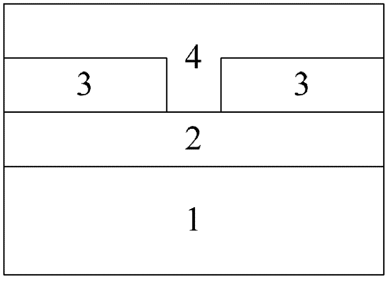
[0027] The structure of the phase change memory in this example is a "T" type structure, an edge contact structure, a symmetrical structure or an asymmetrical structure.
[0028] (1) Clean the substrate:
[0029] Sonicate the silicon oxide substrate in acetone for 3 minutes, wash it in absolute ethanol and deionized water, blow dry the substrate with a nitrogen gun, and bake it on a hot plate at 103 degrees Celsius to remove moisture on the substrate .
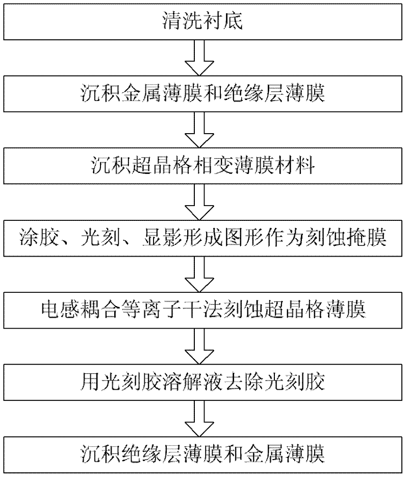
[0030] (2) Deposit metal film and insulating layer film:
[0031] Apply photoresist on the surface of a clean substrate, bake it on a hot plate at 97 degrees Celsius for 3 minutes, select the pattern required on the photolithography mask board, expose it for 30 seconds, and then bake it on a hot plate at 112 degrees Celsius for 110 seconds. After flood exposure for 30 seconds and soaking in the developer for 20 seconds, the required photoresist pattern is formed. Then use magnetron sputtering to deposit a 150nm thick TiW fi...
example 2~5
[0047] The key of the inventive method lies in steps (3) and (5), and all the other steps are basically the same as the prior art, and the metal thin film in steps (2), (7) is Pt or Au or TiW or Ag of 30nm~200nm or Cu or Al or TiN, the insulating layer film is 30nm ~ 200nm SiO 2 or Si 3 N 4 ; In the photolithography process of process step (4), the baking time is 1-10 minutes, the exposure time is 1-8 minutes, and the developing time is 1-5 minutes; removing photoresist in process step (6) is Soak in acetone for 1 to 2 hours, then sonicate for 5 to 10 minutes. The photolithography process includes optical lithography, electron beam lithography and nanoimprint lithography. The inductively coupled plasma dry etching gas contains Cl 2 , HBr, BCl 3 Mixed gas of halogen element gas such as Ar and inert gas such as Ar. The substrate can be a silicon dioxide substrate, a silicon substrate, a gallium arsenide substrate, etc.
[0048] The method of the present invention i...
PUM
| Property | Measurement | Unit |
|---|---|---|
| Thickness | aaaaa | aaaaa |
Abstract
Description
Claims
Application Information