

Zinc oxide micro-nano array and preparation method thereof
A zinc oxide array, micro-nano technology, applied in the direction of zinc oxide/zinc hydroxide, nanotechnology, etc., can solve difficult micro, nano device structure, and it is difficult to realize the controllable positioning device growth of zinc oxide nanostructure, method Limiting problems such as chemical and physical vapor deposition, to achieve the effect of wide range of uses, simple preparation process and strong operability
- Summary
- Abstract
- Description
- Claims
- Application Information
AI Technical Summary
Problems solved by technology
Method used
Image

Examples
Embodiment 1
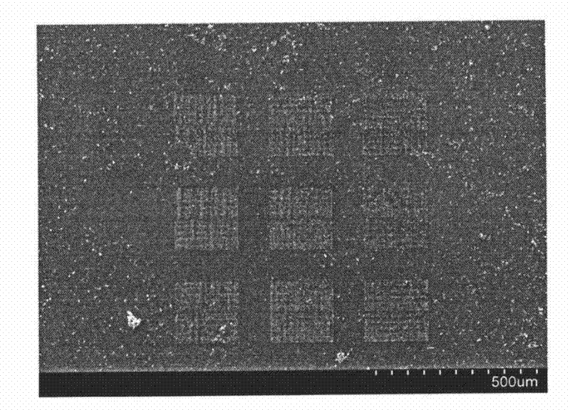
[0027] This example is used to illustrate the preparation method of the zinc oxide micro-nano array provided by the present invention.
[0028] 1) Preparation of precursor solution: 3 grams of Zn(NO 3 ) 2 ·6H 2 O (0.1mol / L) and 0.7 g (CH 2 ) 6 N 4 (0.05mol / L) was added to 100ml deionized water, and kept stirring for at least 10 minutes until the solution was uniform;
[0029] 2) Prepare the substrate: select a silicon wafer with a smooth surface as the substrate, after ultrasonic cleaning, thermally evaporate metal zinc on the silicon wafer, and feed high-temperature oxygen to make it react to form a zinc oxide film (thickness of the film 45 nanometers); after the substrate is cooled, spray a layer of photoresist with a thickness of 45 nanometers on the film (MJB4 contact alignment exposure system produced by SUSS in Germany; technical indicators: resolution 0.7 microns 365 nanometers light source, The alignment accuracy is 0.5 microns), and then partial electron beam ex...
Embodiment 2
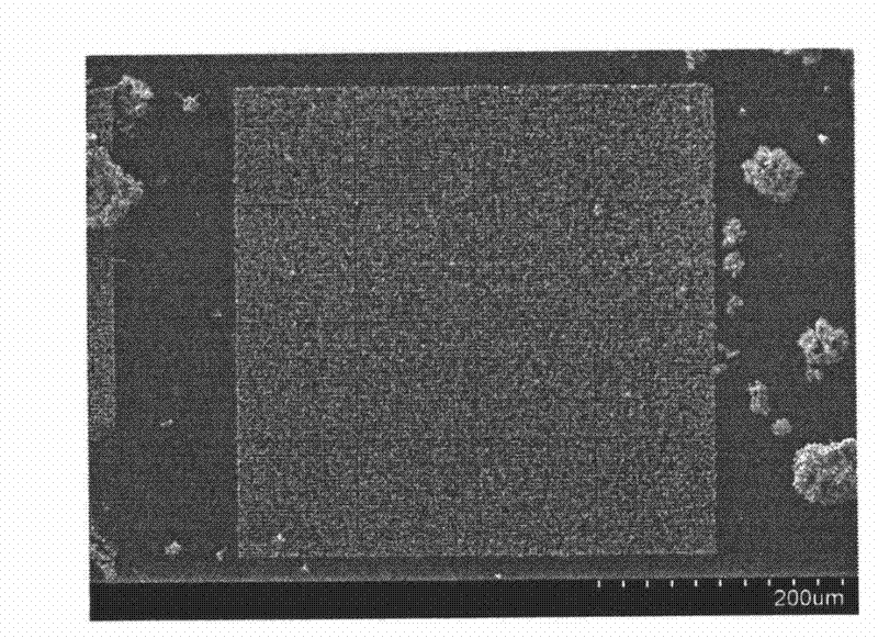
[0033] This example is used to illustrate the preparation method of the zinc oxide micro-nano array provided by the present invention.
[0034] 1) Preparation of precursor solution: 0.3 g of Zn(NO 3 ) 2 ·6H 2 O (0.01mol / L) and 0.14 grams (CH 2 ) 6 N 4 (0.01mol / L) was added to 100ml deionized water, and kept stirring for at least 10 minutes until the solution was uniform;
[0035] 2) Prepare the substrate: select a silicon wafer with a flat and smooth surface as the substrate, after ultrasonic cleaning, evaporate a layer of zinc oxide film (45 nanometers in thickness) on the silicon wafer by magnetron sputtering; wait for the substrate to cool Finally, on the thin film, the photoresist (same as example 1) that one layer of thickness is sprayed on the film is 45 nanometers, then carries out local electron beam exposure on the photoresist, obtains the hole array that average aperture is 300 nanometers;
[0036] 3) Form a zinc oxide array: put the substrate prepared in step 2)...
Embodiment 3
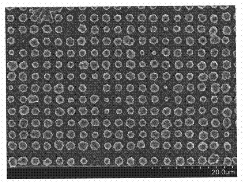
[0039] This example is used to illustrate the preparation method of the zinc oxide micro-nano array provided by the present invention.
[0040] 1) Preparation of precursor solution: 3 grams of Zn(NO 3 ) 2 ·6H 2 O (0.1mol / L) and 0.14 g (CH 2 ) 6 N 4 (0.01mol / L) was added to 100ml deionized water, and kept stirring for at least 10 minutes until the solution was uniform;
[0041] 2) Prepare the substrate: select a silicon wafer with a smooth surface as the substrate, after ultrasonic cleaning, thermally evaporate metal zinc on the silicon wafer, and feed high-temperature oxygen to make it react to form a zinc oxide film (thickness of the film is 15 nanometers); after the substrate is cooled, a layer of photoresist (same as example 1) with a thickness of 45 nanometers is sprayed on the film, and then partial electron beam exposure is carried out on the photoresist to obtain an average aperture of 300 nanometers array of holes;
[0042] 3) Form a zinc oxide array: put the su...
PUM
| Property | Measurement | Unit |
|---|---|---|
| Average pore size | aaaaa | aaaaa |
| The average diameter | aaaaa | aaaaa |
| Length | aaaaa | aaaaa |
Abstract
Description
Claims
Application Information