

Electrochemical preparation process of Cu2ZnSnS4 film
A preparation process and electrochemical technology, applied in metal material coating process, electrolytic inorganic material coating, ion implantation coating, etc., can solve the problems of complex process, deviation of components from ideal chemical ratio, lack of deep understanding of microscopic physical mechanism, etc. , to achieve the effect of simple operation
- Summary
- Abstract
- Description
- Claims
- Application Information
AI Technical Summary
Problems solved by technology
Method used
Image

Examples
Embodiment Construction
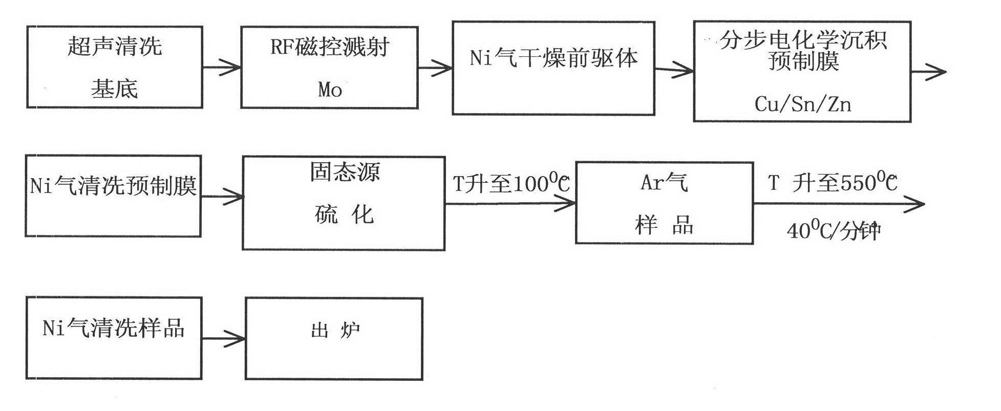
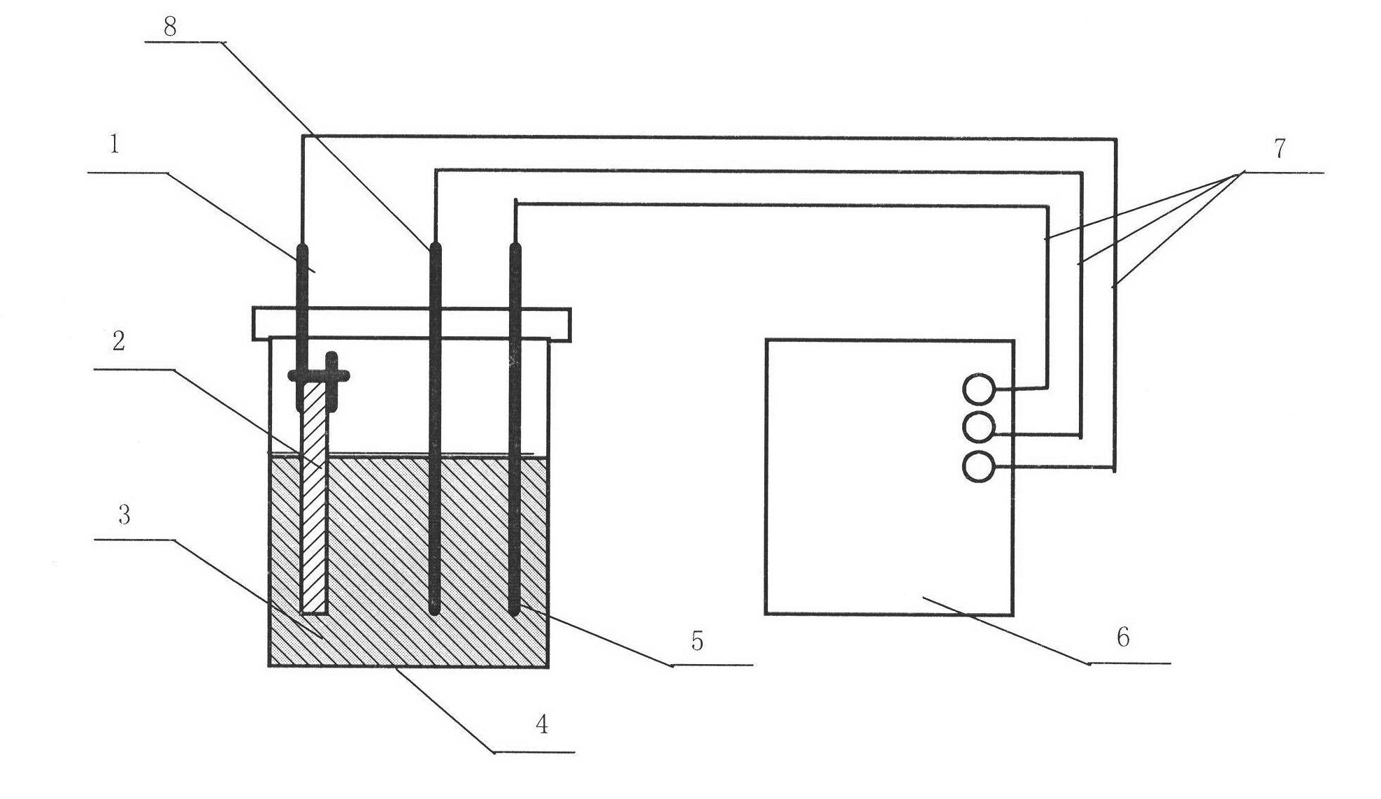
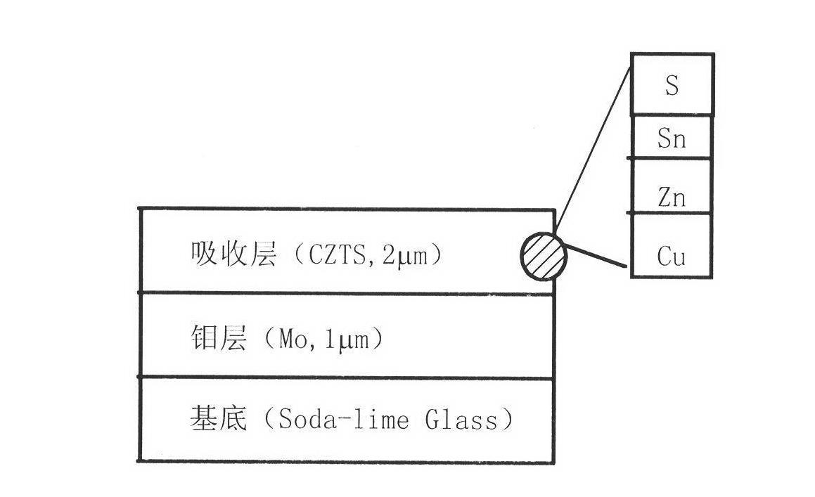
[0012] (1) Soda-lime glass substrate (10mm×10mm) was ultrasonically cleaned with detergent, distilled water, isopropanone and ethanol for 10 minutes, and then dried with nitrogen gas (flow rate 0.1m3 / h) for 5 minutes;
[0013] (2) Mask the edge of the soda-lime glass substrate with polytetrafluoroethylene (PTFE), and deposit a molybdenum layer (precursor) with a thickness of 1 μm on the substrate by radio frequency (RF) magnetron sputtering;
[0014] (3) prepare three kinds of electrolytic solutions of A, B and C respectively with deionized water and metal salt (purity is 99.99wt%): A electrolytic solution is to contain 1.5 moles of sodium hydroxide (NaOH), 50 millimoles of copper chloride ( CuCl2) and 0.1 mole sorbitol (sorbitol) alkaline solution; B electrolyte is a solution containing 0.15 mole zinc chloride (ZnCl2) and buffered by hydrogen ions with a pH value of 3; C electrolyte is a solution containing 2.25 mole hydroxide Sodium (NaOH), an alkaline solution of 55 mmoles...
PUM
 Abstract
Description
Claims
Application Information