Microfluidic atom cavity, on-chip atomic clock chip and preparation method

An atomic cavity and microfluidic technology, applied in the field of MEMS manufacturing, can solve the problems of optical window pollution, influence, low performance of atomic cavity, etc., and achieve the effect of low cost and simple method.

Inactive Publication Date: 2012-06-27
SOUTHEAST UNIV
View PDF5 Cites 11 Cited by
  • Summary
  • Abstract
  • Description
  • Claims
  • Application Information

AI Technical Summary

Problems solved by technology

[0004] Some chip-level atomic clocks are currently designed. In the structure of silicon-glass-silicon, substances such as rubidium chloride and barium azide are directly reacted to form rubidium, and the reaction residue barium chloride stays in the atomic cavity, which will affect the optical window. Pollution will seriously affect the interaction between rubidium, cesium and other substances and light, so the performance of the obtained atomic cavity is not high

Method used


Image

  • Microfluidic atom cavity, on-chip atomic clock chip and preparation method
  • Microfluidic atom cavity, on-chip atomic clock chip and preparation method
  • Microfluidic atom cavity, on-chip atomic clock chip and preparation method

Examples


Embodiment 1

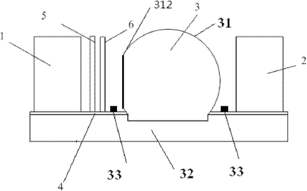
[0039] A microfluidic atomic cavity, a silicon substrate with a microfluidic groove and a borosilicate glass assembly wafer corresponding to the microfluidic groove to form a glass microcavity structure are bonded to form a closed system, the closed system includes a glass atomic cavity , The reactant blocks the micro-channel and the reactant micro-cavity, the reactant micro-cavity is placed with the reactant particles necessary for the generation of the atomic clock, the glass atomic cavity and the reactant micro-cavity are connected through the reactant-blocked micro-channel, bonding The caliber of the reactant glass microcavity on the surface is smaller than the caliber of the glass atomic cavity, the minimum width of the reactant blocking microflow channel is not greater than the minimum particle diameter of the reactant particle, and the glass atomic cavity is provided with a light incident plane.

[0040] In the above technical solution, the reactant blocking micro-channe...

Embodiment 2

[0042] A method for preparing a microfluidic atomic cavity, comprising the following steps: etching a microfluidic groove on a silicon substrate, which is composed of a reactant groove, a reactant blocking microfluidic path and an atomic groove, wherein the diameter of the reactant groove is smaller than The caliber of the atomic tank, the reactant tank and the atomic tank are connected through the reactant barrier micro-channel, the reactant particles are placed in the reactant tank, and then the above-mentioned silicon substrate etched with the micro-channel tank and borosilicate The glass assembly wafers are anodically bonded to form a sealed cavity; a silicon wafer mold is placed vertically on the surface of the borosilicate glass assembly wafer of the above-mentioned bonded wafers at a position corresponding to the microgroove, and then heated in the air to 820 °C ℃ ~ 900 ℃, keep warm for 10 ~ 20min, the reactant particles release gas so that the glass corresponding to the...

Embodiment 3

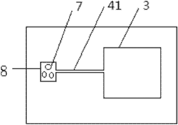
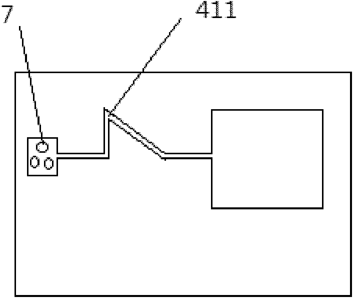
[0045] A miniature atomic clock chip, comprising a laser generator, a filter, a quarter wave plate, a laser detector and the miniature atomic cavity with a light incident plane described in Embodiment 1, a laser generator, a filter, a quarter wave plate A wave plate laser detector is assembled on a borosilicate glass assembly wafer, and their centers are located on the same optical axis as the center of the glass microcavity. The laser generator is located on the side of the airtight glass atomic cavity with a light incident plane. A filter and a quarter-wave plate are arranged sequentially between the laser generator and the light incident plane. The laser light emitted by the laser generator passes through the filter and the quarter-wave plate, and enters the airtight glass atomic cavity through the light incident plane. After being emitted again, it is detected by a laser detector, and a heater is arranged around the glass microcavity, and the above-mentioned heater, laser g...


PUM


Abstract

The invention discloses a microfluidic atom cavity, an on-chip atomic clock chip and a preparation method. The method includes steps: a silicon substrate with a microfluidic channel and a borosilicate glass assembly wafer with a glass microcavity structure corresponding to the microfluidic channel are bonded to form a closed system, the closed system comprises a glass atom cavity, a reactant partition microfluidic channel and a reactant microcavity, reactant particles of materials necessarily required by atomic clock generation are arranged in the reactant microcavity, the glass atom cavity is communicated with the reactant microcavity through the reactant partition microfluidic channel, the aperture of the reactant microcavity on a bonding surface is smaller than that of the glass atom cavity, the minimum width of the reactant partition microfluidic channel is no larger than the minimum particle diameter of the reactant particles, and the glass micro cavity is provided with a light incidence plane. The smaller microcavity containing the reactant powder is connected with the larger microcavity required by forming of the spherical glass microcavity, forming of a spherical rubidium steam cavity and sealing of gas can be completed at one step, fine sealing performance is achieved, no impurities can be led in, performance of an atomic clock can be improved, the spherical rubidium steam cavity can be integrated into a microchip-level atomic clock system, planar packaging of the atomic clock can be realized, and size of the atomic clock is reduced effectively.

Description

technical field [0001] The invention relates to a MEMS (micro-electro-mechanical system) manufacturing technology, in particular to a method for preparing a small-volume, low-cost, good-tightness, high-stability wafer-level spherical rubidium vapor chamber capable of mass production. Background technique [0002] At present, atomic clocks are the most accurate artificial clocks, and the accuracy of atomic clocks can reach one billionth of a second or even higher. A special type of quantum transition in atomic clocks is the hyperfine transition, which involves the interaction of the nuclear magnetic field of the atom and the magnetic field of the electrons outside the nucleus. In principle, the principle of atomic clocks is basically clear, and there are two main directions for current development: one is to improve the performance of atomic clocks in terms of accuracy; the other is to miniaturize them while ensuring their performance. Currently, the world's most accurate at...

Claims


Application Information

Patent Timeline
Patent Type & Authority Applications(China)
IPC IPC(8): B81B7/00B81C1/00G04F5/14
Inventor 尚金堂魏文龙秦顺金蒯文林于慧王亭亭
Owner SOUTHEAST UNIV
Why Eureka
Try Eureka