Copper drawing and electroplating method for plastic substrate
A technology of plastic base material and wire drawing, which is applied in the direction of sputtering plating, ion implantation plating, vacuum evaporation plating, etc., can solve the problems of polluting the natural ecological environment, large environmental pollution, waste of water resources, etc., to reduce environmental and Harm to human beings, reduction of production cost, effect of reduction of waste water discharge
- Summary
- Abstract
- Description
- Claims
- Application Information
AI Technical Summary
Problems solved by technology
Method used
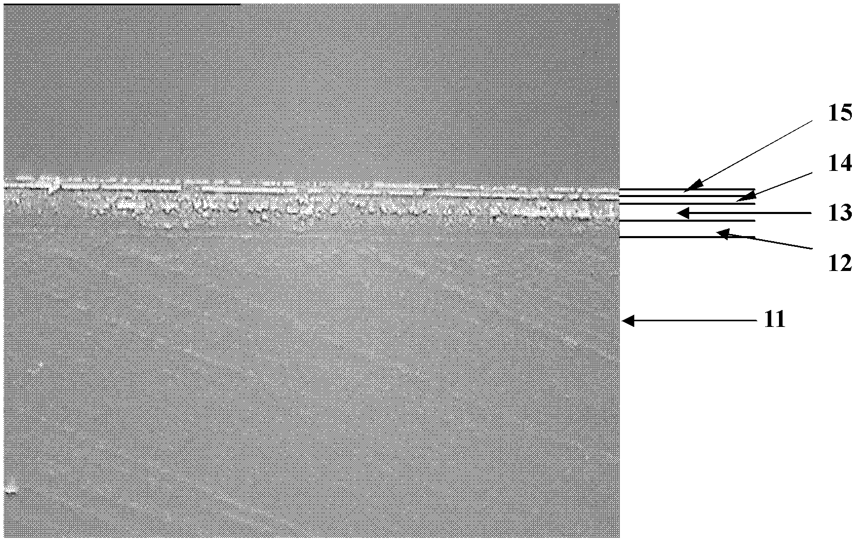
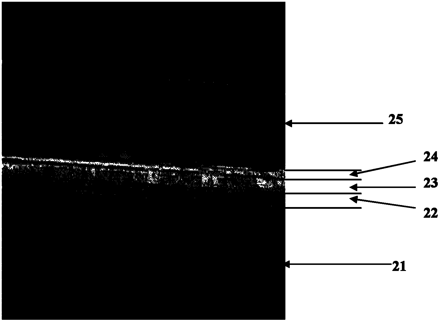
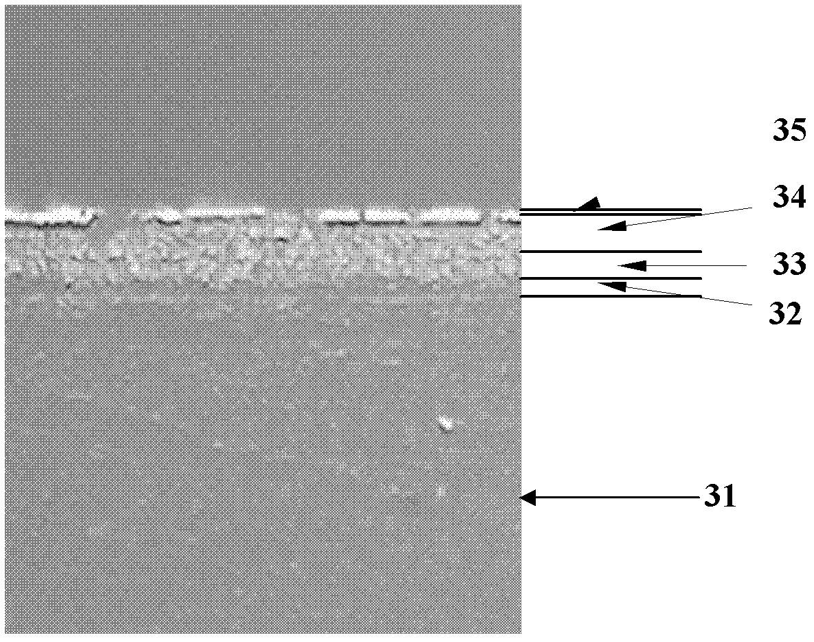
Image

Examples
Embodiment 1
[0051] (1) Pretreatment of modified PP plastic substrate
[0052] Implement dry cleaning method on the modified PP plastic substrate, use plasma flame treatment and then carry out electrostatic treatment to remove oil and dust on the surface of the modified PP plastic substrate;
[0053] (2) PVD (Physical Vapor Deposition) metallization of plastic substrates
[0054] Perform PVD (Physical Vapor Deposition) metallization on the modified PP plastic substrate, and implement PVD plasma modification, metal plating bottom layer, metal transition layer and metal conductive layer in sequence. The plasma modification process conditions are ion source current 0.5A, Bias voltage 80V, duty cycle 80%, argon flow rate 50SCCM, oxygen flow rate 50SCCM, furnace vacuum pressure 0.2Pa, activation time 5min to achieve the purpose of cleaning and activating the substrate surface, metallized bottom layer, metal transition layer and metal conductive The layer adopts a high-power intermediate freque...
Embodiment 2
[0074] (1) Pretreatment of ABS plastic substrate
[0075] Implement dry cleaning method on the ABS plastic substrate, and use hydrocarbon vacuum cleaning to remove the oil stain on the surface of the ABS plastic substrate;
[0076] (2) PVD (Physical Vapor Deposition) metallization of plastic substrates
[0077] Perform PVD (Physical Vapor Deposition) metallization on the ABS plastic substrate, and implement PVD plasma modification, metal plating bottom layer, metal transition layer and metal conductive layer in sequence. The plasma modification process conditions are ion source current 0.3A, bias voltage 150V, duty cycle 80%, argon flow rate 50SCCM, oxygen flow rate 80SCCM, furnace vacuum pressure 0.3Pa, activation time 6min to achieve the purpose of cleaning and activating the surface of the substrate, metal-plated bottom layer, metal transition layer and metal conductive layer are Using high-power intermediate frequency pulse power supply, metal plating bottom current is 30...
Embodiment 3
[0097] (1) Pretreatment of modified PP plastic substrate
[0098] Implement dry cleaning method on the modified PP plastic substrate, use plasma flame treatment and then carry out electrostatic treatment to remove oil and dust on the surface of the modified PP plastic substrate;
[0099] (2) PVD (Physical Vapor Deposition) metallization of plastic substrates
[0100]PVD (Physical Vapor Deposition) metallization is carried out on the modified PP plastic substrate, and PVD plasma modification, metal plating bottom layer, metal transition layer and metal conductive layer are carried out in sequence. The plasma modification process conditions are ion source current 0.3A, Bias voltage 150V, duty cycle 50%, argon flow rate 100SCCM, oxygen flow rate 10SCCM, vacuum pressure in the furnace 0.2Pa, activation time 10min to achieve the purpose of cleaning and activating the surface of the substrate, metallized bottom layer, metal transition layer and metal conduction The layer adopts a h...
PUM
 Abstract
Description
Claims
Application Information
 - R&D
- Intellectual Property
- Life Sciences
- Materials
- Tech Scout
- Unparalleled Data Quality
- Higher Quality Content
- 60% Fewer Hallucinations
Browse by: Latest US Patents, China's latest patents, Technical Efficacy Thesaurus, Application Domain, Technology Topic, Popular Technical Reports.
© 2025 PatSnap. All rights reserved.Legal|Privacy policy|Modern Slavery Act Transparency Statement|Sitemap|About US| Contact US: help@patsnap.com