Catalyst for zinc oxide nanowire growth, and application of catalyst
A technology of zinc oxide nanowires and catalysts, applied in zinc oxide/zinc hydroxide, physical/chemical process catalysts, catalyst activation/preparation, etc., can solve the problems of limiting the application of nanowire materials and the high temperature of zinc oxide nanowire growth
- Summary
- Abstract
- Description
- Claims
- Application Information
AI Technical Summary
Problems solved by technology
Method used
Image
Examples
Embodiment 1
[0044] A catalyst used for the growth of zinc oxide nanowires is an Au / Ga double-layer film formed by the mass ratio of metal Au and metal Ga, that is, Au: Ga is 1.5:1;
[0045] The preparation method of the catalyst Au / Ga bilayer film used for the growth of the above-mentioned a kind of zinc oxide nanowire is as follows:
[0046] Using a-plane Al 2 o 3 As the substrate material, a 1nm gallium layer is plated on the substrate by electron beam evaporation with an evaporation rate of 0.01A / s, and then a 1.5nm gold layer is plated on the substrate by an electron beam evaporation method with an evaporation rate of 0.01A / s s.
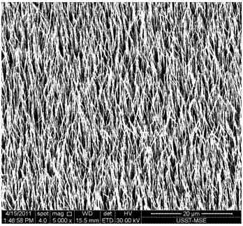
[0047] a-surface Al treated by electron evaporation as described above 2 o 3 As the substrate material, ZnO nanowires are grown by chemical vapor deposition, the specific process is as follows:
[0048] (1) Fully grind zinc oxide nanopowder with equal mass ratio and graphite powder passing through a 300 mesh sieve, and put them into a quartz boat;
[0...
Embodiment 2
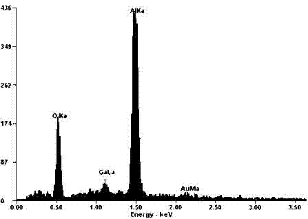
[0057] First, the a-plane Al 2 o 3 A 1.5nm-thick Au film was plated on the substrate, and then local Ga ions were implanted by focused ion beam etching (FIB). The ion beam etching conditions were: accelerating voltage 30kV, beam current 0.19nA, etching The time is 70ms, and the size of the etching area is a circle with a diameter of 20um. Electron energy dispersive spectroscopy (EDS) of Ga+ implanted Au thin films in the region after focused ion beam etching as image 3 shown, from image 3 It can be seen that the peak of Ga appeared in the EDS spectrum, indicating that Ga was successfully implanted into the Au film.
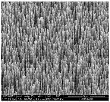
[0058] a-side Al treated with FIB 2 o 3 As the substrate material, ZnO nanowires are grown by chemical vapor deposition, and the specific growth process is as follows:
[0059] (1) Fully grind zinc oxide nanopowder with equal mass ratio and graphite powder passed through a 300-mesh sieve, and put them into a quartz boat;
[0060] (2), the a-face Al ...
Embodiment 3
[0067] c-plane Al 2 o 3 As the substrate, 1.5nm Au film as the catalyst, the catalyst film is locally treated with FIB technology for local Ga ion implantation, the ion beam etching conditions are acceleration voltage 30kV, beam current size 0.19nA, etching time 70ms, etching area The size is a circle with a diameter of 20um.
[0068] c-plane Al treated with FIB 2 o 3 As the substrate material, ZnO nanowires are grown by chemical vapor deposition, and the specific growth process is as follows:
[0069] (1) Fully grind zinc oxide nanopowder with equal mass ratio and graphite powder passing through a 300 mesh sieve, and put them into a quartz boat;
[0070] (2) The c-plane Al coated with the catalyst Au / Ga alloy film used for the growth of zinc oxide nanowires obtained by ion implantation 2 o 3 The substrate is placed on the powder in the quartz boat;
[0071] (3) Put the quartz boat into the quartz glass tube, then put the quartz glass tube into the tube furnace, and ali...
PUM
| Property | Measurement | Unit |
|---|---|---|
| Evaporation rate | aaaaa | aaaaa |
Abstract
Description
Claims
Application Information


