Copper indium diselenide solar cell and production method thereof

A technology of solar cells and copper indium selenide, which is applied in the manufacture of circuits, electrical components, and final products, can solve problems such as uneven composition and crystal phase, difficult control of ingredients, and high manufacturing costs, so as to improve photoelectric conversion efficiency and improve composition Effects that are easy to control and low in production cost

Inactive Publication Date: 2012-07-11
HELIOHAWK OPTOELECTRONICS CORP
View PDF2 Cites 4 Cited by
  • Summary
  • Abstract
  • Description
  • Claims
  • Application Information

AI Technical Summary

Problems solved by technology

[0002] In copper indium gallium solar cells, the key lies in the process of making copper indium gallium selenide thin films or copper indium gallium selenide sulfur thin films. Usually, in the production process of copper indium gallium selenide thin films, sputtering copper indium gallium alloy targets, co-sputtering Copper gallium alloy target material and indium target material, co-sputtering copper gallium alloy target material and copper indium alloy target material, etc., to produce copper indium gallium thin film, followed by selenization step or further vulcanization to make copper indium gallium selenide Thin film or copper indium gallium selenide sulfur thin film, the process needs to pass selenium vapor, selenium hydride or hydrogen sulfide at high temperature, which are poisonous gases to the human body, and have potential industrial safety hazards during the process and mechanical maintenance
[0003] In addition, the manufacturing process of this method takes a

Method used


Image

  • Copper indium diselenide solar cell and production method thereof
  • Copper indium diselenide solar cell and production method thereof
  • Copper indium diselenide solar cell and production method thereof

Examples


Embodiment Construction

[0031] The implementation of the present invention will be described in more detail below with reference to the drawings and component symbols, so that those skilled in the art can implement it after reading this specification.

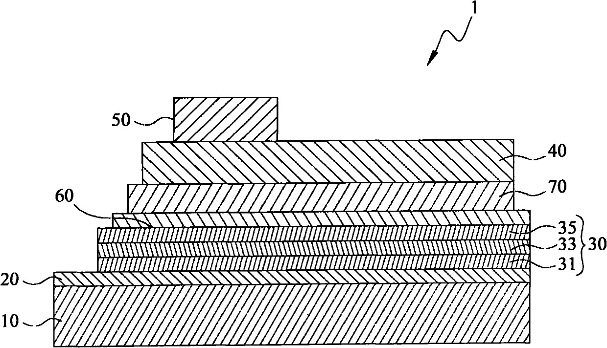
[0032] refer to figure 1 , Schematic diagram of the structure of the copper indium selenide solar cell of the present invention. Such as figure 1 As shown, the CISe solar cell 1 of the present invention includes a substrate 10 , a back metal electrode 20 , a light absorbing layer 30 , a transparent conductive layer 40 and a contact electrode layer 50 . The substrate 10 can be silicon wafer, glass, acrylic, rigid polymer substrate or flexible polymer substrate. The back metal electrode 20 is formed on the substrate 10 and is formed of a highly reflective metal material, preferably molybdenum (Mo). The light-absorbing layer 30 is formed on the back metal electrode 20 and includes a plurality of light-absorbing films, such as figure 1 The first light...


PUM


Abstract

The invention discloses a copper indium diselenide solar cell and a production method thereof, wherein the solar cell comprises a substrate, a back metal electrode, a light absorption layer, a transparent electric conduction layer and a contact electrode layer, the light absorption layer comprises a plurality of copper indium gallium diselenide films or copper indium gallium diselenide sulfur compound films which have different atom ratios, different target materials can be directly sputtered into a film on the back metal electrode in a direct current or radio frequency mode during the production process, so selenylation does not need to be carried out, the copper indium diselenide solar cell is safer, has high efficiency and costs less for production, components are easy to control, crystalline phases are single, the concentration is uniform, and the conversion efficiency is also improved.

Description

technical field [0001] The invention relates to a copper indium selenium solar cell and a manufacturing method thereof. Background technique [0002] In copper indium gallium solar cells, the key lies in the process of making copper indium gallium selenide thin films or copper indium gallium selenide sulfur thin films. Usually, in the production process of copper indium gallium selenide thin films, sputtering copper indium gallium alloy targets, co-sputtering Copper gallium alloy target material and indium target material, co-sputtering copper gallium alloy target material and copper indium alloy target material, etc., to produce copper indium gallium thin film, followed by selenization step or further vulcanization to make copper indium gallium selenide Thin film or copper indium gallium selenide sulfur thin film, the process needs to pass selenium vapor, selenium hydride or hydrogen sulfide at high temperature, which are poisonous gases to the human body, and have potentia...

Claims


Application Information

Patent Timeline
IPC IPC(8): H01L31/032H01L31/18
CPCY02P70/50
Inventor 钟润文
Owner HELIOHAWK OPTOELECTRONICS CORP
Why Eureka
Try Eureka