Thin-film solar photovoltaic cell with nano wire array structure and preparation method for thin-film solar photovoltaic cell

A technology of nanowire arrays and thin-film solar energy, which is applied in the manufacture of circuits, electrical components, and final products. It can solve the problems of difficult large-area production and preparation, high preparation costs, and difficult control of the microstructure of element ratio materials, and achieve convenient large-area Application, low preparation cost, and the effect of reducing the probability of hole and electron recombination

Inactive Publication Date: 2012-07-11
SUN YAT SEN UNIV
View PDF7 Cites 27 Cited by
  • Summary
  • Abstract
  • Description
  • Claims
  • Application Information

AI Technical Summary

Problems solved by technology

The main common problems are that it is difficult to achieve large-scale production and preparation, the preparation cost is high, and the ratio of each element and the microstructure of the material are difficult to control

Method used


Image

  • Thin-film solar photovoltaic cell with nano wire array structure and preparation method for thin-film solar photovoltaic cell
  • Thin-film solar photovoltaic cell with nano wire array structure and preparation method for thin-film solar photovoltaic cell

Examples


Embodiment 1

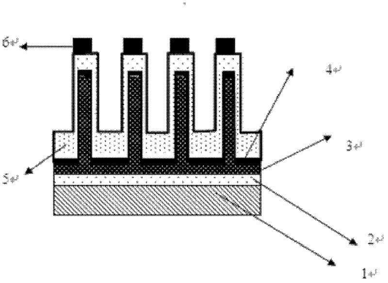
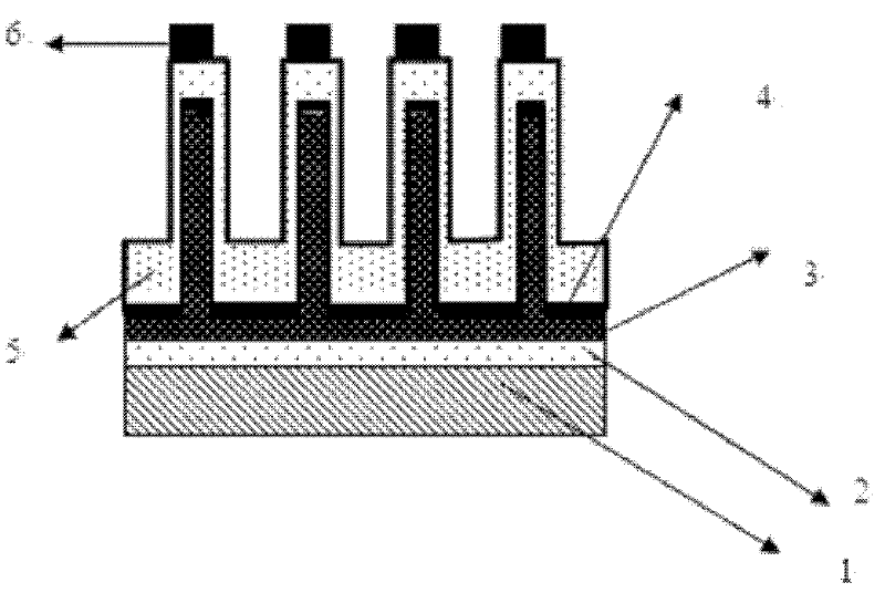
[0034] This example chooses CuInS 2 As the composition of the semiconductor nanowire array, CdS as the n-type layer, infiltration as the means of depositing cadmium sulfide layer, Al-doped ZnO layer as the window layer, thermal evaporation as the deposition of In, Al-doped ZnO layer, metal grid electrode, back The means of electrode and copper film, the back electrode is made of Mo, the metal grid electrode is made of Ti, and the substrate is made of glass.

[0035] Specific steps are as follows:

[0036] (1) After cleaning with 1mol / L NaOH solution and 1mol / L hydrochloric acid solution respectively, deposit a Mo layer with a thickness of 800nm ​​on the glass substrate which has been ultrasonically cleaned in sequence with absolute ethanol and deionized water ;

[0037] (2) evaporating a layer of copper film with a thickness of 10um on the substrate after thermal evaporation deposition of Mo;

[0038] (3) Put the substrate with the copper film evaporated obtained in step (2...

Embodiment 2

[0045] This example selects Cu(In, Ga)(S, Se) 2 As the composition of the semiconductor nanowire array, CdS is used as the n-type layer, the aluminum-doped zinc oxide layer is used as the window layer, spin coating is used as the means of depositing the cadmium sulfide layer, and magnetron sputtering is used as the deposition of In, Ga, Se, aluminum-doped zinc oxide layer , Metal grid electrode, back electrode and copper film, the back electrode is made of Al, the metal grid electrode is made of Cu, and the substrate is made of silicon wafer.

[0046] Specific steps are as follows:

[0047] (1) After cleaning with 1mol / L NaOH solution and 1mol / L hydrochloric acid solution, a layer of Al is deposited on the silicon wafer substrate that has been ultrasonically cleaned with absolute ethanol and deionized water in sequence, and the thickness of Al is 800nm ;

[0048] (2) Sputter a layer of copper film with a thickness of about 1um on the substrate after Al is deposited by magnet...

Embodiment 3

[0056] In this example, Cu(In 0.7 , Ga 0.3 )(Se,S) 2 As the composition of the semiconductor nanowire array, ZnS is used as the n-type layer, the aluminum-doped zinc oxide layer is used as the window layer, and the chemical bath is used as the means of depositing ZnS. Electron beam evaporation is used as a means of depositing In, Ga, Se, aluminum-doped zinc oxide layer, metal grid electrode, back electrode and copper film. W is used for the back electrode, Ni is used for the metal grid electrode, and mica is used for the substrate.

[0057] Specific steps are as follows:

[0058] (1) Deposit a layer of W on the newly cut mica sheet substrate, and the thickness of W is 800nm;

[0059] (2) On the substrate after electron beam evaporation W, evaporate a layer of copper film with a thickness of about 1um;

[0060] (3) Put the substrate with the copper film evaporated obtained in step (2) into a reactor, and after 10 minutes of passing through a mixed gas with a volume ratio of...


PUM

PropertyMeasurementUnit
diameteraaaaaaaaaa
lengthaaaaaaaaaa
thicknessaaaaaaaaaa

Abstract

The invention discloses a method for preparing a thin-film solar photovoltaic cell with a copper indium gallium selenide (CIGS) nano wire array structure. The method comprises the following steps of: growing a large-area cuprous sulfide or copper sulfide nano wire array by adopting a gas-solid reaction method, and converting the cuprous sulfide or copper sulfide nano wire array into a CIGS nano wire array by physical vapor deposition and heat treatment methods. The component, the phase structure and the energy band structure of the semiconductor nano wire array can be regulated by controlling the categories of deposition elements, the deposition sequence, the deposition process, post treatment and the like, so that solar photovoltaic cells with different structures and properties are prepared. Through the cell, light reflection is reduced, light absorption is increased, the probability of producing current carriers can be increased, the probability of recombination of holes and electrons is reduced, and the photoelectric conversion efficiency is greatly improved. The method is low in cost, the preparation processes are controllable, the prepared nano wire array is uniform in structure distribution, and preparation of the nano structural thin-film solar photovoltaic cell with large area and high photoelectric conversion efficiency can be realized.

Description

technical field [0001] The invention belongs to the technical field of solar photovoltaic cells, in particular to a thin-film solar photovoltaic cell with a CIGS nanowire array structure and a preparation method thereof. Background technique [0002] With the continuous increase of human demand for energy, non-renewable energy such as coal, oil, and natural gas will face a crisis of shortage. In addition, these energy sources also have their own shortcomings. They are easy to cause environmental pollution, acid rain, greenhouse effect and other problems, which threaten the survival and development of human beings. The development and utilization of new energy and renewable energy is imperative. [0003] Solar cells can directly convert solar energy and electrical energy, and are a subject of more concern in the development and utilization of solar energy. Its application can change the current situation of energy shortage and help to reduce the environmental pollution cause...

Claims


Application Information

Patent Timeline
Patent Type & Authority Applications(China)
IPC IPC(8): H01L31/18H01L31/0352C23C14/22C23C14/06C23C14/18
CPCY02P70/50
Inventor 任山李立强刘珠凤李明洪澜
Owner SUN YAT SEN UNIV
Why Eureka
Try Eureka