Nanometer structure copper zinc tin sulfide (CZTS) film photovoltaic cell and preparation method of nanometer structure CZTS film photovoltaic cell

A thin-film photovoltaic cell and nanostructure technology, applied in photovoltaic power generation, circuits, electrical components, etc., can solve the problems of low conversion efficiency of CZTS thin-film solar photovoltaic cells, and achieve high photoelectric conversion efficiency, improved band gap adjustment, and simple preparation process. Effect

Inactive Publication Date: 2012-08-15
SUN YAT SEN UNIV
View PDF7 Cites 15 Cited by
  • Summary
  • Abstract
  • Description
  • Claims
  • Application Information

AI Technical Summary

Problems solved by technology

[0010] The above-mentioned methods can prepare CZTS films with high quality and good uniformity, but the conversion efficiency of the CZTS thin film solar photovoltaic cells is low, which is not only lower than the photoelectric conversion efficiency of 9.66% of the CZTS thin film solar cells prepared in the laboratory, but also Far below the theoretical conversion efficiency

Method used


Image

  • Nanometer structure copper zinc tin sulfide (CZTS) film photovoltaic cell and preparation method of nanometer structure CZTS film photovoltaic cell
  • Nanometer structure copper zinc tin sulfide (CZTS) film photovoltaic cell and preparation method of nanometer structure CZTS film photovoltaic cell

Examples


Embodiment 1

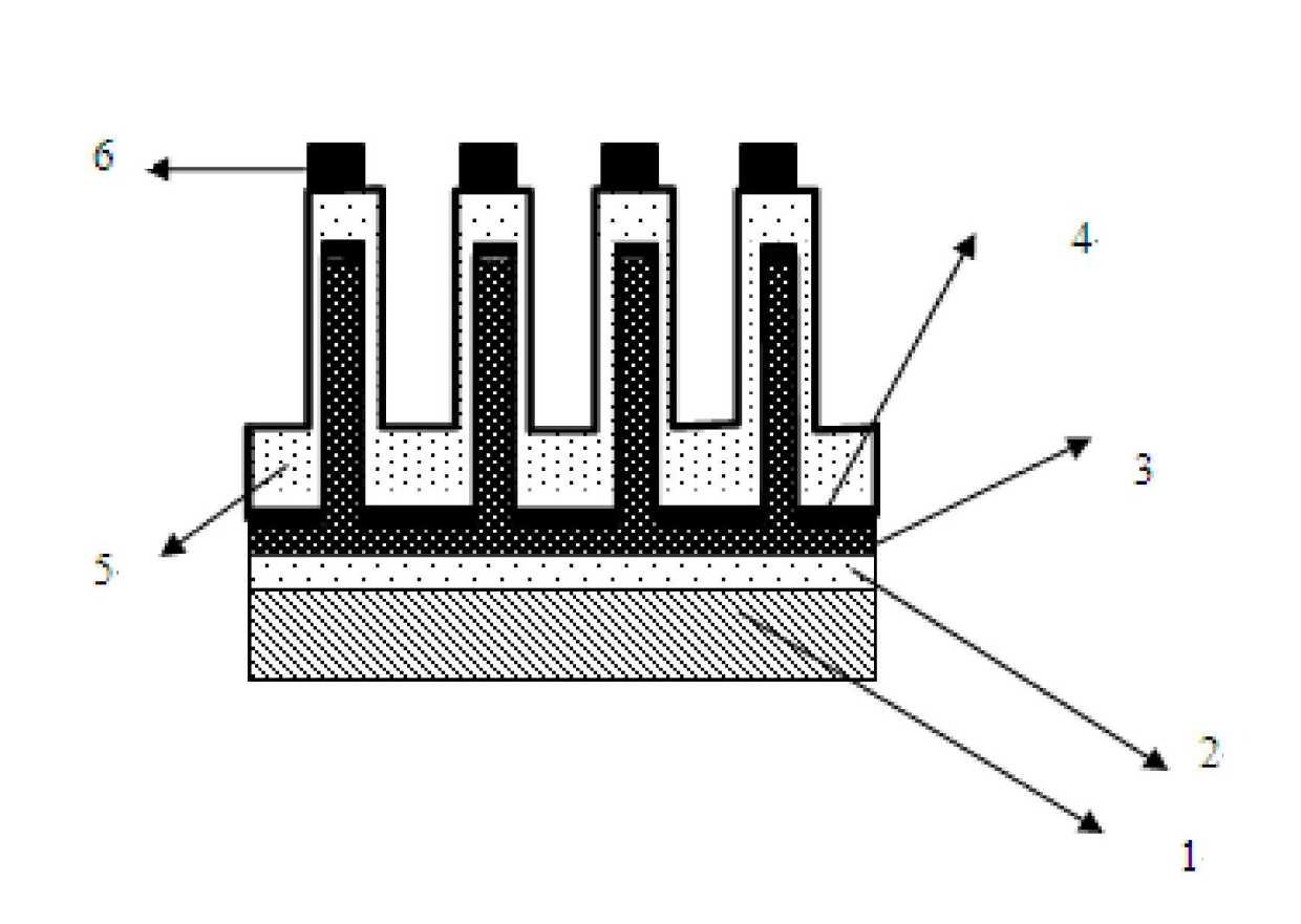
[0047] A nanostructure CZTS thin film photovoltaic cell, prepared by the following steps:

[0048] (1) Take the ceramics, wash them with 1mol / L NaOH solution and 1mol / L hydrochloric acid solution in turn, then ultrasonically clean them with absolute ethanol and deionized water in turn, and then sputter a layer of ITO on the ceramic substrate. The thickness is 700nm (ITO glass can also be used);

[0049] (2) Sputter a layer of copper film with a thickness of 1um on the substrate after sputtering deposition of ITO (ITO glass can also be selected);

[0050] (3) Mix the substrate sputtered with copper film with hydrogen sulfide / oxygen mixed gas (the volume ratio of the two is 1:4), and vulcanize at 18°C ​​for 18 hours to form a cuprous sulfide nanowire array;

[0051] (4) Put the substrate on which the cuprous sulfide nanowire array has been formed into 0.5 mol / L hydrochloric acid aqueous solution to dissolve the surface oxide layer;

[0052] (5) The product of step (4) was soak...

Embodiment 2

[0060] A nanostructure CZTS thin film photovoltaic cell, prepared by the following steps:

[0061] (1) Take the silicon wafer, wash it with 1mol / L NaOH solution and 1mol / L hydrochloric acid solution in turn, then ultrasonically clean it with absolute ethanol and deionized water in turn, and then sputter a layer of Al on the silicon wafer substrate, The thickness of Al is 800nm;

[0062] (2) Sputter a layer of copper film with a thickness of about 1um on the substrate after Al is deposited;

[0063] (3) Mix the substrate sputtered with copper film with hydrogen sulfide / oxygen mixed gas (the volume ratio of the two is 1:2), and vulcanize at 20°C for 14 hours to form a subnano-sulfide array;

[0064] (4) Put the substrate on which the copper sulfide nanowire array was formed into 1mol / L hydrochloric acid aqueous solution to dissolve the surface oxide layer;

[0065] (5) Put the product of step (4) on the rotating substrate holder of the magnetron sputtering apparatus, co-sputte...

Embodiment 3

[0072] A nanostructure CZTS thin film photovoltaic cell, prepared by the following steps:

[0073] (1) Electron beam evaporation of a layer of W on the newly cut mica substrate, the thickness of W is 800nm;

[0074] (2) Evaporate a layer of copper film with a thickness of about 1um on the substrate after electron beam evaporation of W;

[0075] (3) Mix the substrate with the evaporated copper film with hydrogen sulfide / oxygen mixed gas (the volume ratio of the two is 1:2), and vulcanize at 22°C for 12 hours to form a copper sulfide nanowire array;

[0076] (4) Put the substrate on which the copper sulfide nanowire array was formed into 1mol / L hydrochloric acid aqueous solution to dissolve the surface oxide layer;

[0077] (5) Put the product of step (4) on the rotating substrate holder, layer-evaporate Zn, Sn, S, and then 2 Under gas protection, p-type semiconductor nanowire arrays were obtained after heat treatment at 600°C for 15 hours;

[0078] (6) After the evaporation ...


PUM

PropertyMeasurementUnit
thicknessaaaaaaaaaa
thicknessaaaaaaaaaa
thicknessaaaaaaaaaa

Abstract

The invention discloses a nanometer structure copper zinc tin sulfide (CZTS) film photovoltaic cell, which sequentially consists of a substrate, a back electrode, a p type semiconductor nanometer wire array, an n type semiconductor thin layer, a window layer and a metal grid electrode, wherein the p type semiconductor nanometer wire array consists of semiconductor alloy (CuxB<1-x>)2Cy(DzS<1-z>), wherein x is greater than 0 but is smaller than or equal to 1, y is greater than or equal to 0 but smaller than or equal to 2, z is greater than or equal to 0 but smaller than 1, B is silver and/or gold, C is more than one kind of materials of aluminum, zinc or tin, D is selenium and/or tellurium. Through the subsequent processes of controlling the deposition element types, the deposition element sequence, the heat treatment mode and the like, the ingredients, the phase structure and the energy band structure of the absorption layer nanometer wire array are regulated, so the solar photovoltaic cells with different structures and performance can be prepared. The nanometer structure CZTS film photovoltaic cell provided by the invention has the advantages that the light reflection is reduced, good light capture capability is realized, the band gap regulation is improved, and the great improvement of the photoelectric conversion efficiency is finally realized.

Description

technical field [0001] The invention belongs to the technical field of solar photovoltaic cells, and in particular relates to a nanostructure CZTS thin film photovoltaic cell and its preparation method and application. Background technique [0002] The survival and development of human beings are inseparable from energy and the environment. With the rapid development of the world economy, the energy crisis and environmental problems are becoming increasingly severe, and become one of the major problems that human beings urgently need to solve in the 21st century. Therefore, the importance of developing clean and renewable energy is becoming increasingly prominent. Solar energy is inexhaustible and inexhaustible clean energy. Sunlight covers a wide range of the entire earth. As long as there is sun, we can use solar energy to generate electricity. [0003] At present, the solar cells used in the market are still dominated by monocrystalline silicon / polycrystalline silicon c...

Claims


Application Information

Patent Timeline
Patent Type & Authority Applications(China)
IPC IPC(8): H01L31/0352H01L31/072H01L31/18
CPCY02E10/50Y02P70/50
Inventor 任山李明李立强刘珠凤洪澜
Owner SUN YAT SEN UNIV
Why Eureka
Try Eureka