Method for preparing superconductive nanometer device by negative electron beam resist exposure process

A technology of electron beam resist and nano-devices, which is applied in metal material coating technology, technology for producing decorative surface effects, decorative art, etc., can solve the difficulties of making fine lines and dense graphics, electrodes and device ohms Poor contact performance, difficulty in obtaining high-quality samples, etc., to achieve the effect of facilitating electrical measurement, improving efficiency and material utilization, and increasing selection ratio

Active Publication Date: 2012-09-05
INST OF PHYSICS - CHINESE ACAD OF SCI
View PDF5 Cites 11 Cited by
  • Summary
  • Abstract
  • Description
  • Claims
  • Application Information

AI Technical Summary

Problems solved by technology

For hard metal and ceramic high-temperature superconducting thin films, it is difficult to obtain high-quality samples by exfoliation and desorption
Positive photoresist PMMA, ZEP520, etc. are also used as etching masks in the research, but it will be difficult to make fine lines and dense patterns; at the same time, this method generally needs to make measurement bridges through ultraviolet exposure first, and then through electron beam exposure. Complex process for making nanostructures
In addition, in literature reports, there is also a method of directly processing superconducting devices by using maskless

Method used


Image

  • Method for preparing superconductive nanometer device by negative electron beam resist exposure process
  • Method for preparing superconductive nanometer device by negative electron beam resist exposure process
  • Method for preparing superconductive nanometer device by negative electron beam resist exposure process

Examples


Embodiment 1

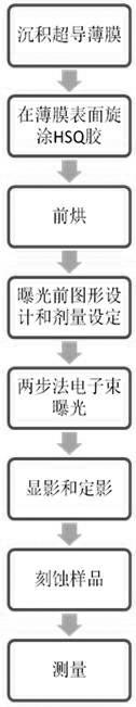
[0060] with SiO 2 Superconducting Nb (niobium) thin films deposited on substrates, electron beam resist HSQ exposure process

[0061] 1. In insulating SiO 2 On the substrate, a superconducting Nb thin film was deposited by magnetron sputtering with a thickness of about 50 nm;

[0062] 2. Use a diamond knife or a wire cutting machine to divide the film into 10mm × 10mm size films;

[0063] 3. Remove debris and other contaminants on the surface of the film by ultrasonic cleaning. After cleaning, use N 2 air dry

[0064] 4. Spin-coat HSQ resist on the surface of the film without pre-spraying, directly accelerate to 4000rpm, rotate for one minute, and the thickness of the glue is about 120nm;

[0065] 5. After the spin coating is completed, place it on a hot plate with a temperature of 170°C and bake for 3 minutes;

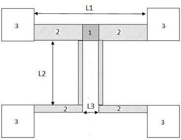
[0066] 6. As image 3 As shown, the fine structure area and the bridge area belong to different layers (I, II), and doses are set for different areas of the exp...

Embodiment 2

[0080] Fabrication of nanoscale superconducting devices—superconducting nano-SQUIDs.

[0081] with SiO 2 Superconducting Nb (niobium) thin films deposited on substrates, electron beam resist HSQ exposure process

[0082] 1. In insulating SiO 2 On the substrate, a superconducting Nb thin film was deposited by magnetron sputtering with a thickness of about 50 nm;

[0083] 2. Use a diamond knife or a wire cutting machine to divide the film into 10mm × 10mm size films;

[0084] 3. Remove debris and other contaminants on the surface of the film by ultrasonic cleaning. After cleaning, use N 2 air dry

[0085]4. Spin-coat HSQ resist on the surface of the film without pre-spraying, directly accelerate to 4000rpm, rotate for one minute, and the thickness of the glue is about 120nm;

[0086] 5. After the spin coating is completed, place it on a hot plate with a temperature of 170°C and bake for 3 minutes;

[0087] 6. Design the exposure pattern of the fine structure region as Fi...


PUM

PropertyMeasurementUnit
Thicknessaaaaaaaaaa
Line widthaaaaaaaaaa
Lattice constantaaaaaaaaaa

Abstract

The invention discloses a method for preparing a superconductive nanometer device by a negative electron beam resist exposure process. The method mainly comprises the following steps of: spinning a hydrogen silsesquioxane (HSQ) resist on a superconductive thin film; pre-drying; designing an exposure graph; exposing by two steps; developing; fixing; and etching. By using the method, the superconductive nanometer device which is stable in performance and uniform in line width and has the minimum line width of 15 nm can be prepared. Residues do not exist in an electrode region after the etching step is performed by setting an exposure amount in different regions and changing the thickness of an exposure product in the corresponding region, so that electrical measurement is facilitated. HSQ has high anti-etching performance and is suitable to serve as an etching mask of a hard superconductive metal material, so that the etching selection ratio can be increased. An electrode and the device are obtained through one-time etching; no contact potential difference exists between the electrode and the device; and the success rate of the device is high. Furthermore, a plurality of independent micro electric bridges are exposed on the same thin film, so that the efficiency of integrating and measuring the electric bridges can be improved, and the material utilization rate is increased; and the superconductive nanometer device has great significance for research on nanometer structures made of rare materials.

Description

technical field [0001] The invention belongs to the technical field of micro-nano processing, in particular to a method for preparing a superconducting nano-device by a negative electron beam resist exposure process. Background technique [0002] With the development of micro- and nano-fabrication technology, the research on superconducting materials at the micro-scale has attracted extensive attention. Novel superconducting nanodevices are constantly emerging, such as nano-superconducting quantum interferometers (nano-SQUID), superconducting nanowire single-photon detectors (SNSPD), Josephson junctions, and superconducting qubits (Quantum bits) Wait. In the fabrication process of superconducting devices, it is required not only to have a small size, but also to minimize the influence of micro-nano processing on superconducting properties. This is the key to obtaining high-performance devices, and it is also a difficulty. [0003] In the preparation of traditional supercon...

Claims


Application Information

Patent Timeline
IPC IPC(8): B81C1/00
Inventor 张伟君杨海方何世坤顾长志邱祥冈
Owner INST OF PHYSICS - CHINESE ACAD OF SCI
Why Eureka
Try Eureka