
Non-refrigeration infrared detector

An uncooled infrared and detector technology, applied in the direction of electric radiation detectors, manufacturing microstructure devices, piezoelectric devices/electrostrictive devices, etc., can solve the problem of pixel failure, large difference in thermal insulation performance, and influence on correction effects, etc. question

Active Publication Date: 2012-09-26
ZHEJIANG DALI TECH
View PDF4 Cites 40 Cited by
  • Summary
  • Abstract
  • Description
  • Claims
  • Application Information

AI Technical Summary

Problems solved by technology

The first type of blind element is a structure that itself absorbs infrared radiation but conducts heat well with the substrate (US006507021). This blind element can better eliminate the influence of substrate temperature changes, but due to its thermal insulation performance is quite different from that of the pixel, Cannot eliminate the Joule heating effect of electrical bias during detection
[0011] The second blind element has the same thermal insulation performance as the pixel, but the blind element does not absorb infrared light by setting an infrared reflective layer on the upper surface of the blind element.
The disadvantages of this method are: first, if one (group) of blind cells is damaged, it will directly cause a column of pixels to fail to work; There is a large difference in the pixels at the far end; third, when there is a temperature gradient in the detector substrate, the temperature felt by the blind element cannot correctly represent the actual temperature of the pixels under different temperature gradients, which will directly affect the correction effect ; Fourth, even if the blind element is designed to have exactly the same structure as the pixel, due to the non-uniformity of the manufacturing process, the blind element cannot completely eliminate the non-uniformity of the pixel

Method used


Image

  • Non-refrigeration infrared detector
  • Non-refrigeration infrared detector
  • Non-refrigeration infrared detector

Examples


Embodiment Construction

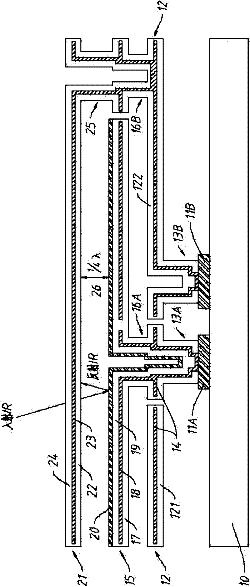
[0092] attached figure 1 It is a cross-sectional view of the first detector microbridge structure provided by the present invention, including:

[0093] The semiconductor substrate 10 is characterized by including various circuits (not explicitly shown in the figure) for signal detection of the uncooled detector, commonly referred to in the industry as a readout circuit (ROIC). The substrate 10 is generally made of single crystal silicon, but other semiconductor materials can also be used. The readout circuit is generally fabricated by a CMOS process.

[0094] The metal plates 11A and 11B for the electrical connection between the micro-bridge structure and the ROIC are generally made of CMOS materials such as aluminum or aluminum alloys, copper, and tungsten. The metal discs 11A and 11B can be completed together with the ROIC through a CMOS process, or can be implemented during the detector processing process. in the attached figure 1 Four metal discs are set up in total, ...


PUM


Abstract

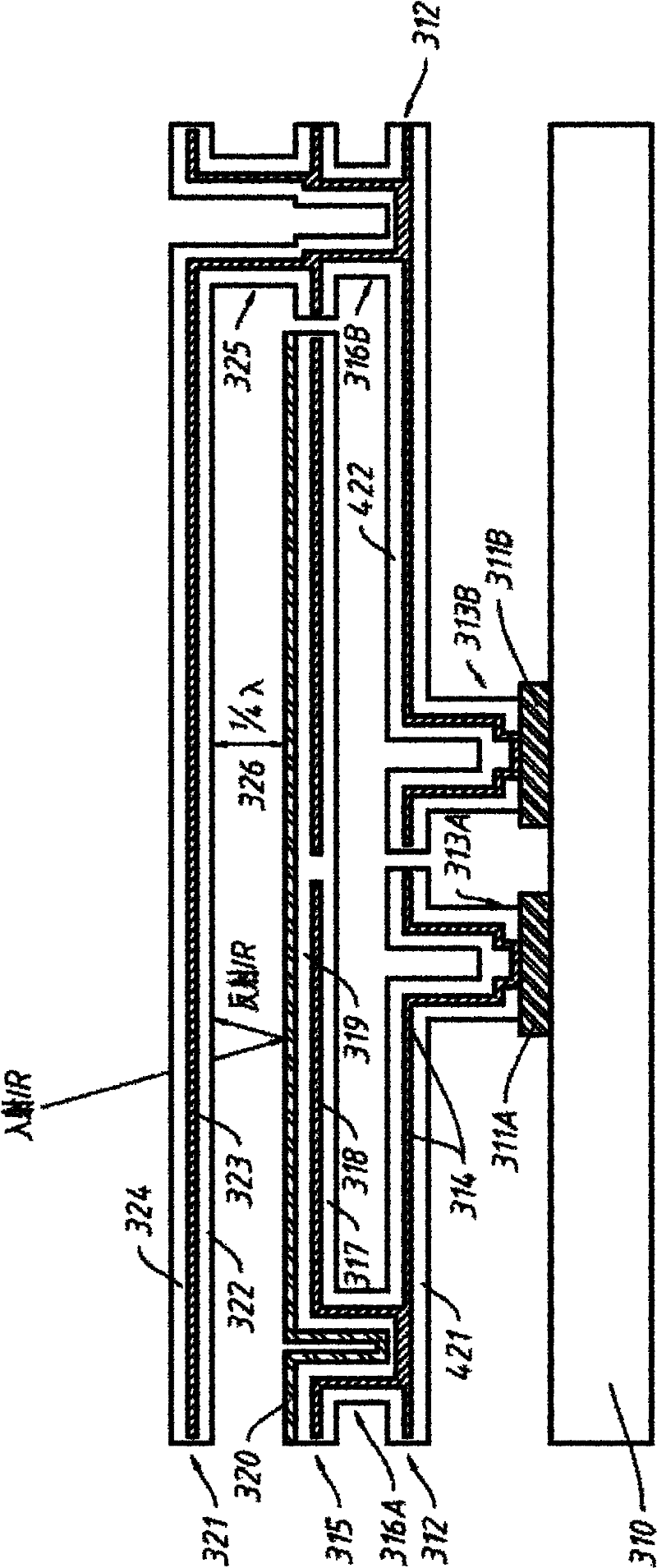
The invention discloses a non-refrigeration infrared detector, and especially disclsoes a microbridge structure and a two-dimension focal plane array comprised of the microbridge structure. The microbridge structure includes a semiconductor substrate, a cantilever beam hierarchic microstructure made above the substrate, a blind pixel hierarchic microstructure made above the substrate, and a pixel hierarchic microstructure made above the blind pixels and the cantilever beam. The pixels and the blind pixels are integrated at the same position on the substrate in the microbridge structure in a three-dimensional way, so the disadvantage of the pixels and the blind pixels being in different temperature gradients due to being at different positions far from each other on the substrate in conventional non-refrigeration infrared detectors is effectively avoided. The one-to-one corresponding relationship of the pixels and the blind pixels is realized using the above focal plane detector with the microbridge structures, and the one-to-one corresponding relationship will effectively improve a background correction function of the non-refrigeration detector and has great help in improving the performance of the detector.

Description

[0001] technical field [0002] The invention belongs to the field of micro-electromechanical systems, in particular to the field of uncooled infrared detectors. [0003] Background technique [0004] According to the working temperature of the chip, infrared detectors are generally divided into two types: cooling type and uncooling type. The cooling type is usually a photodetector made of a narrow bandgap semiconductor. It needs to be cooled by liquid nitrogen to suppress hot carriers and noise during operation. Therefore, the volume and weight are relatively large, and the price is relatively expensive. Uncooled infrared detectors are also called room temperature detectors, which can work at room temperature without refrigeration, so they have the advantages of being more portable. Uncooled infrared detectors are generally thermal detectors, that is, they work by detecting the thermal effect of infrared radiation. Commonly used infrared heat detectors include thermopile...

Claims


Application Information

Patent Timeline
IPC IPC(8): G01J5/10B81B3/00B81C1/00
Inventor 姜利军刘海涛潘峰钱良山池积光
Owner ZHEJIANG DALI TECH
Learn More