Single crystal graphene pn node and preparation method thereof

A single crystal graphene, pn junction technology, applied in graphene, single crystal growth, single crystal growth, etc., can solve the problems of unfavorable scale expansion, poor use stability, etc., and achieve high mobility and high photoelectric conversion efficiency Effect

Active Publication Date: 2013-03-06
PEKING UNIV
View PDF1 Cites 30 Cited by
  • Summary
  • Abstract
  • Description
  • Claims
  • Application Information

AI Technical Summary

Problems solved by technology

The current methods for preparing graphene single crystal pn junctions are often based on micron-scale graphene obtained by mechanical exfoliation, which is not conduc...

Method used


Image

  • Single crystal graphene pn node and preparation method thereof
  • Single crystal graphene pn node and preparation method thereof
  • Single crystal graphene pn node and preparation method thereof

Examples


Embodiment 1

[0040] Example 1, single modulation to prepare single-level single-crystal graphene pn junction

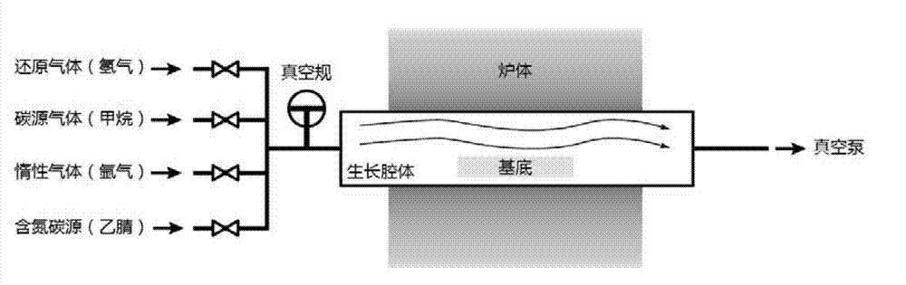
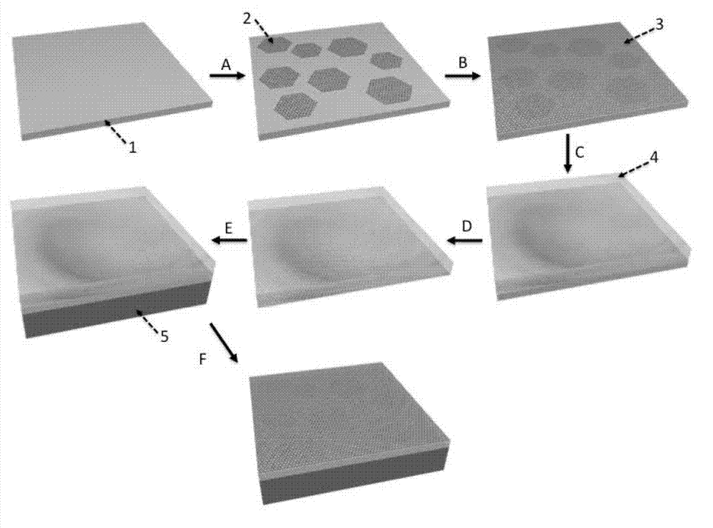
[0041]1) Use 5% dilute hydrochloric acid and deionized water to clean the copper foil (produced by Alfa Aesar, with a purity of 99.8%, and a thickness of 25 μm) in sequence, and place the copper foil in a sleeve with a magnetic control device, and then place the sleeve The tube is placed in a tube furnace, and the temperature of the furnace body is raised to 1020°C under a hydrogen atmosphere with a flow rate of 5 sccm, and the system pressure is about 10 Pa, and kept for 30 minutes;

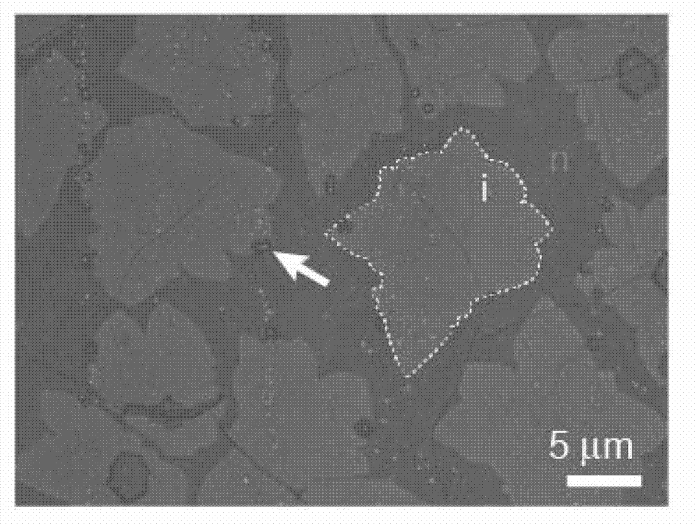
[0042] 2) Lower the temperature of the furnace body to 1000°C, keep the flow rate of hydrogen gas constant, feed methane gas with a flow rate of 5 sccm, keep it for 30 seconds, and the system pressure is about 20 Pa to complete the growth of intrinsic graphene islands, the size of which is 2- 20μm;

[0043] 3) Keep the flow rate of hydrogen gas constant, turn off the methane gas, feed argon gas wit...

Embodiment 2

[0053] Embodiment 2, three-time modulation prepares multilevel graphene pn junction

[0054] 1) step is with embodiment 1 step 1);

[0055] 2) Adjust the temperature of the furnace body to 980°C, keep the flow rate of hydrogen gas constant, feed in methane gas with a flow rate of 5 sccm, keep it for 10 seconds, and the system pressure is about 20 Pa to complete the growth of intrinsic graphene, whose size is 2-5 μm;

[0056] 3) Keep the temperature of the furnace body and the flow rate of hydrogen gas constant, turn off the methane gas, feed in argon gas with a flow rate of 200 sccm, keep it for 3 minutes, and lower the temperature of the furnace body to 900°C while feeding in argon gas;

[0057] 4) Stabilize the temperature of the furnace body at 900°C, keep the hydrogen flow constant, turn off the argon gas, open the needle valve for controlling the acetonitrile vapor, keep the partial pressure of acetonitrile at 5Pa, and grow for 10s to complete the growth of nitrogen-doped...


PUM


Abstract

The invention discloses a single crystal graphene pn node and a preparation method thereof. The modulated and doped graphene pn node is prepared according to the method which comprises the following steps of 1, annealing a copper foil substrate; 2, growing a sub-monolayer intrinsic graphene island on the surface of a copper foil by taking methane as a carbon source; 3, cleaning a growing system by using inert gas; 4, taking acetonitrile steam as a nitrogen-containing carbon source and growing nitrogen doped graphene on the boundary of the intrinsic graphene island; 5, repeating the steps 2, to 4, for at least zero time to obtain the single-level or multi-level graphene pn node; 6, quickly reducing the temperature to stop a growing process; and 7, transferring the graphene pn node which is obtained through modulating, doping and growing onto any target substrate by using polymethyl methacrylate (PMMA) as a medium. The modulated and doped graphene pn node with high quality is obtained by regulating the carbon source in the graphene growing process. The product has very high migration rate and photon to current conversion efficiency; and a transfer characteristic curve of the product has a double-Dirac point, so that the single crystal graphene pn node can be applied to logic devices, such as a phase inverter and a frequency multiplier.

Description

technical field [0001] The invention relates to a single crystal graphene pn junction and a preparation method thereof. Background technique [0002] Graphene is a two-dimensional film material composed of a single layer of carbon atoms arranged in a hexagonal symmetrical honeycomb structure. Due to its excellent properties in electricity, optics, heat and mechanics, graphene has attracted extensive attention in various fields such as physics, chemistry, biology and materials since its discovery, and has also attracted extensive attention from the industry. For electron transport, the electron mobility of graphene is more than two orders of magnitude higher than that of traditional silicon materials, and the symmetrical energy band structure results in matching electron and hole mobility, so graphene is regarded as a silicon-based electronic material. strong contender. In terms of optics, graphene maintains good light transmission in the range from visible light to far inf...

Claims


Application Information

Patent Timeline
IPC IPC(8): C30B25/02C30B29/02C01B31/04C01B32/186C01B32/194
Inventor 刘忠范剡剀吴迪彭海琳
Owner PEKING UNIV
Why Eureka
Try Eureka