Black heterogeneous crystalline cell and manufacture method thereof

A manufacturing method and technology of crystalline silicon, applied in the direction of final product manufacturing, sustainable manufacturing/processing, circuits, etc., can solve the problems of difficulty in covering amorphous silicon, increased surface area of ​​silicon wafers, etc., to achieve simple and easier control, fragmentation rate Low, low thermal stress effect

Inactive Publication Date: 2013-03-27
GD SOLAR
View PDF4 Cites 17 Cited by
  • Summary
  • Abstract
  • Description
  • Claims
  • Application Information

AI Technical Summary

Problems solved by technology

However, texturing leads to a significant increase in the surface area of ​​the silicon wafer, and the surface of the silicon wafer after texturing has a large number of "troughs" and "peaks". If these surfaces are not processed and modified by wet chemical or plasma methods, the 5-15nm Amorphous silicon would have difficulty covering such a surface

Method used


Image

  • Black heterogeneous crystalline cell and manufacture method thereof
  • Black heterogeneous crystalline cell and manufacture method thereof
  • Black heterogeneous crystalline cell and manufacture method thereof

Examples


Embodiment 1

[0036] Embodiment 1, the manufacturing method of black heterogeneous crystalline silicon cell is as follows:

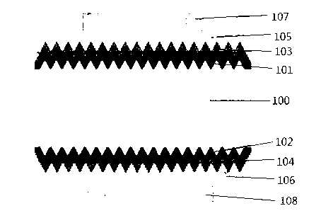
[0037] A. Select an N-type silicon wafer with a resistivity of 1-5ohm.cm; remove the wire damage layer during the silicon wafer cutting process, and the removed thickness is about 5-20um. Depending on the specific silicon wafer cutting process, acid polishing is used to remove the damaged layer (HNO 3 and HF), or alkali polishing process (high concentration of KOH or NaOH); after polishing, the silicon wafer is cleaned to remove surface pollutants, which can be cleaned by RCA process or ozone (O 3 )+HCl / HF for cleaning, and finally dry the silicon wafer in dry nitrogen;

[0038] B. The intrinsic amorphous silicon layer is coated on both sides, and the deposition of the intrinsic amorphous silicon layer adopts the method of plasma enhanced chemical deposition, using SiH 4 and H 2 The mixed gas realizes the coating of amorphous silicon, and the deposition temperatu...

Embodiment 2

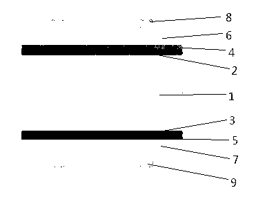
[0043] Embodiment 2, the manufacturing method of the black heterogeneous crystalline silicon battery is the same as that of Embodiment 1, and the specific structure includes the first metal gate line 8, the first polycrystalline boron-doped ZnO thin film 6, the P-type amorphous silicon layer 4, the first intrinsic Amorphous silicon layer 2, a silicon wafer 1, a second intrinsic amorphous silicon layer 3, an N-type amorphous silicon layer 5, a second polycrystalline boron-doped ZnO film 7, and a second metal gate line 9; wherein the intrinsic amorphous The thickness of the silicon layer is 10nm, the thickness of the P-type amorphous silicon layer is 8nm, the thickness of the N-type amorphous silicon layer is 10nm, and the thickness of the positive and negative ZnO conductive films is 1200nm.

Embodiment 3

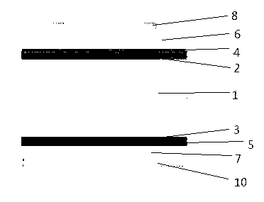
[0044] Embodiment 3, the manufacturing method of the black heterogeneous crystalline silicon battery is the same as that of Embodiment 1, and the specific structure includes the first metal gate line 8, the first polycrystalline boron-doped ZnO thin film 6, the P-type amorphous silicon layer 4, the first intrinsic Amorphous silicon layer 2, a silicon wafer 1, a second intrinsic amorphous silicon layer 3, an N-type amorphous silicon layer 5, a second polycrystalline boron-doped ZnO film 7, and a second metal gate line 9; wherein the intrinsic amorphous The thickness of the silicon layer is 15nm, the thickness of the P-type amorphous silicon layer is 10nm, the thickness of the N-type amorphous silicon layer is 20nm, and the thickness of the positive and negative ZnO conductive films is 2000nm.


PUM

PropertyMeasurementUnit
thicknessaaaaaaaaaa
thicknessaaaaaaaaaa
thicknessaaaaaaaaaa

Abstract

The invention discloses a black heterogeneous crystalline cell which sequentially comprises a first metal electrode, a first conductive film, a P-shaped amorphous silicon layer, a first intrinsic amorphous silicon layer, a silicon wafer, a second intrinsic amorphous silicon layer, an N-shaped amorphous silicon layer, a second conductive film and a second metal electrode. The first conductive film and the second conductive film are polycrystalline boron-doped ZnO films. The manufacture method comprises the steps of preprocessing the surface of the silicon wafer; depositing intrinsic amorphous silicon layer plating in a double-faced mode; depositing the P-shaped amorphous silicon layer from the front side, and depositing the N-shaped amorphous silicon layer from the back side; and growing the ZnO films on the front side and the back side of a cell piece and screen printing metal grid lines on the front sides and the back sides of the conductive films. The polished silicon wafer with the smooth surface is adopted, and light trapping is achieved through pyramid structures of the ZnO films, so that a light trapping structure and surface passivation of the cell can be achieved maximally and respectively, and photoelectric converting efficiency of the cell is improved.

Description

technical field [0001] The invention relates to a solar cell and a manufacturing method thereof, in particular to a black heterogeneous crystal silicon cell and a manufacturing method thereof. Background technique [0002] Since Sanyo started research on amorphous silicon-crystalline silicon heterojunction (HIT) cells, HIT technology has made great progress, and Sanyo has increased the conversion rate of HIT cells to 23.7%, becoming the highest conversion efficiency achieved so far in mass production. One of the tallest crystalline silicon cell structures. Compared with other crystalline silicon batteries, the biggest feature of HIT batteries is the large open circuit voltage (Voc), which benefits from the good passivation effect of amorphous silicon on the surface of crystalline silicon. The above characteristics lead to one of the biggest advantages of HIT batteries, that is, the small temperature coefficient, which can ensure that HIT batteries can obtain more power gene...

Claims


Application Information

Patent Timeline
Patent Type & Authority Applications(China)
IPC IPC(8): H01L31/0747H01L31/0224H01L31/0216H01L31/20
CPCY02E10/50Y02P70/50
Inventor 王明华常辉杨文魁杨帆张杰杨欣陈锐
Owner GD SOLAR
Why Eureka
Try Eureka