Method for preparing epitaxial composite substrate of gallium nitride based semiconducting material

A composite substrate, gallium nitride-based technology, applied in semiconductor/solid-state device manufacturing, electrical components, circuits, etc., can solve the problems of high cost and high lattice mismatch, and achieve low cost, close thermal expansion coefficient, and favorable The effect of heat dissipation

Inactive Publication Date: 2013-04-03
SHANGHAI XINCHU INTEGRATED CIRCUIT
View PDF3 Cites 8 Cited by
  • Summary
  • Abstract
  • Description
  • Claims
  • Application Information

AI Technical Summary

Problems solved by technology

[0005] The invention overcomes the defects of high lattice mismatch or high cost in the prior art, and proposes a method for preparing a gallium nitride-based semiconductor material epitaxial composite substrate

Method used


Image

  • Method for preparing epitaxial composite substrate of gallium nitride based semiconducting material
  • Method for preparing epitaxial composite substrate of gallium nitride based semiconducting material
  • Method for preparing epitaxial composite substrate of gallium nitride based semiconducting material

Examples


preparation example Construction

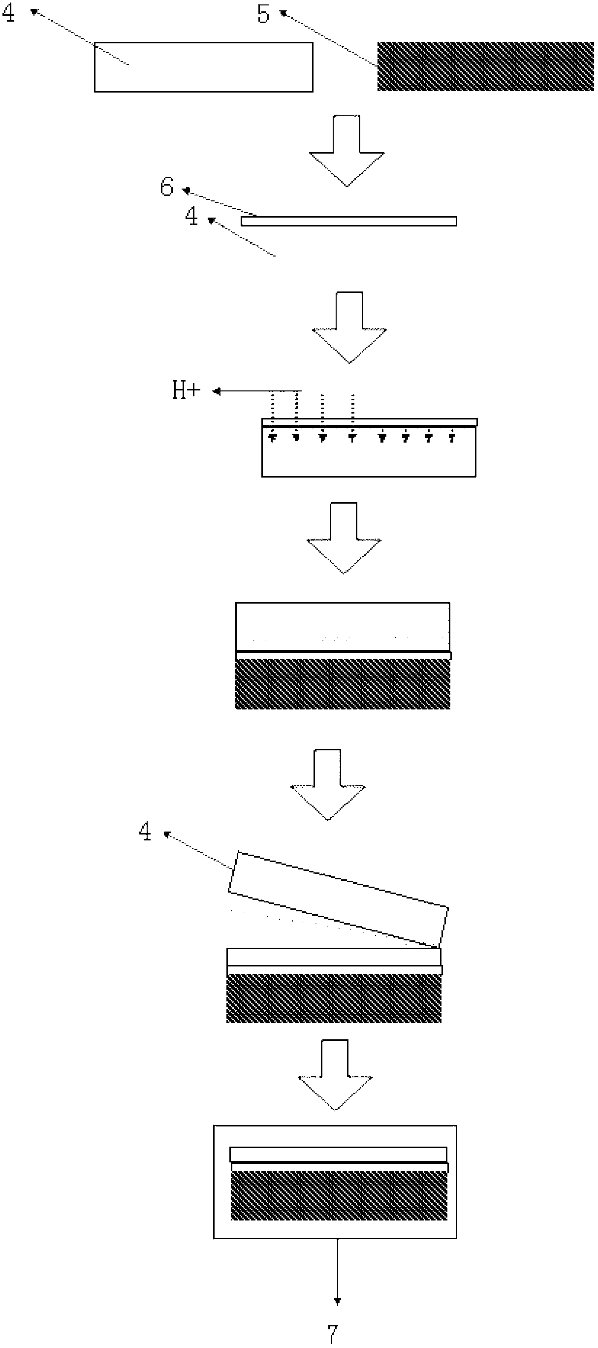
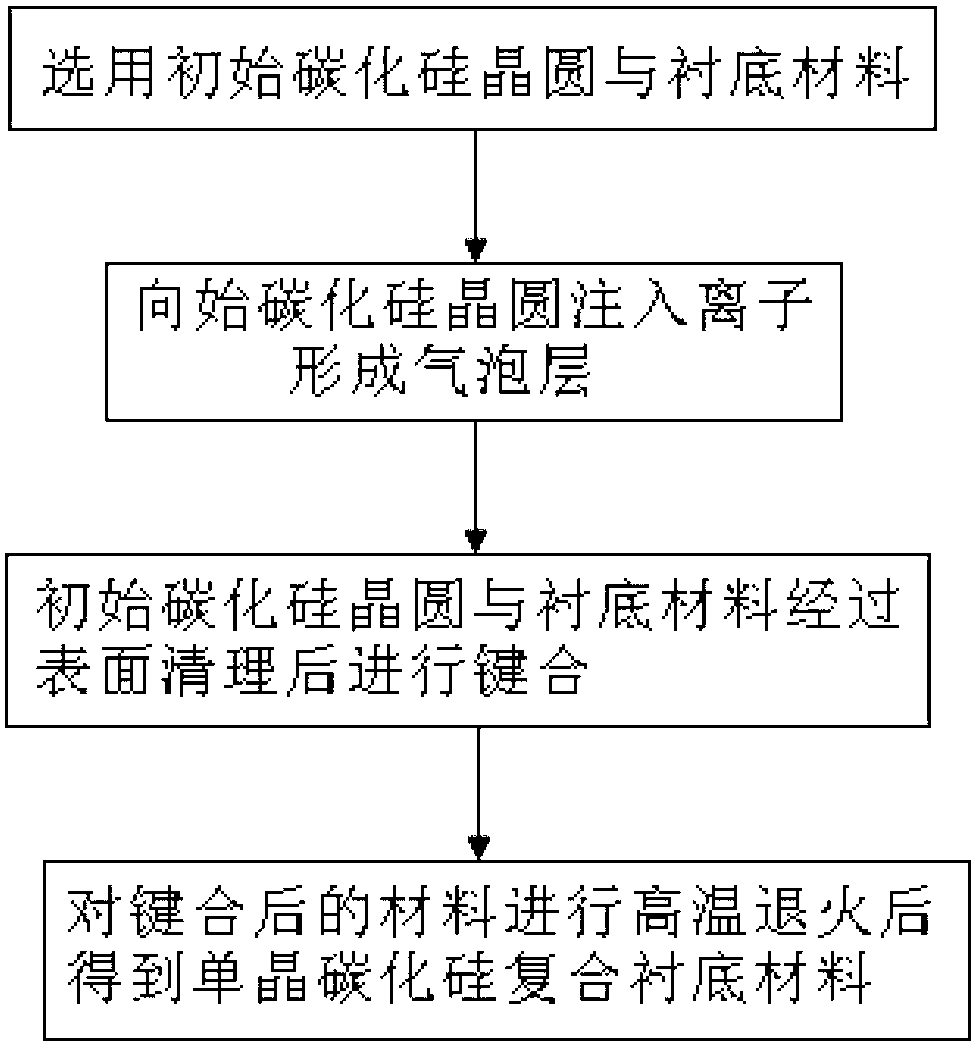
[0026] The preparation method of the GaN-based semiconductor material epitaxial composite substrate of the present invention, such as figure 2 shown, including:

[0027] Step 1: Select an initial single crystal silicon carbide (SiC) wafer 1 and a substrate material 2; the initial single crystal silicon carbide wafer 1 is a 4H or 6H phase single crystal silicon carbide with a diameter of 1 to 6 inches and a thickness of 0.1 to 0.8 mm. The substrate material 2 is a single crystal silicon or polycrystalline silicon wafer with a diameter of 1 to 6 inches, or a disk made of sintered nitride / oxide ceramic powder, with a thickness of 0.2 mm to 1 mm. Nitride ceramic powders include boron nitride and aluminum nitride; oxide ceramic powders include aluminum oxide.

[0028] Step 2: Ion implantation of the hydrogen injection intelligent peeling method, the implantation is hydrogen ions, helium ions or co-implantation of both, or co-implantation of boron ions and hydrogen ions; the impl...

Embodiment

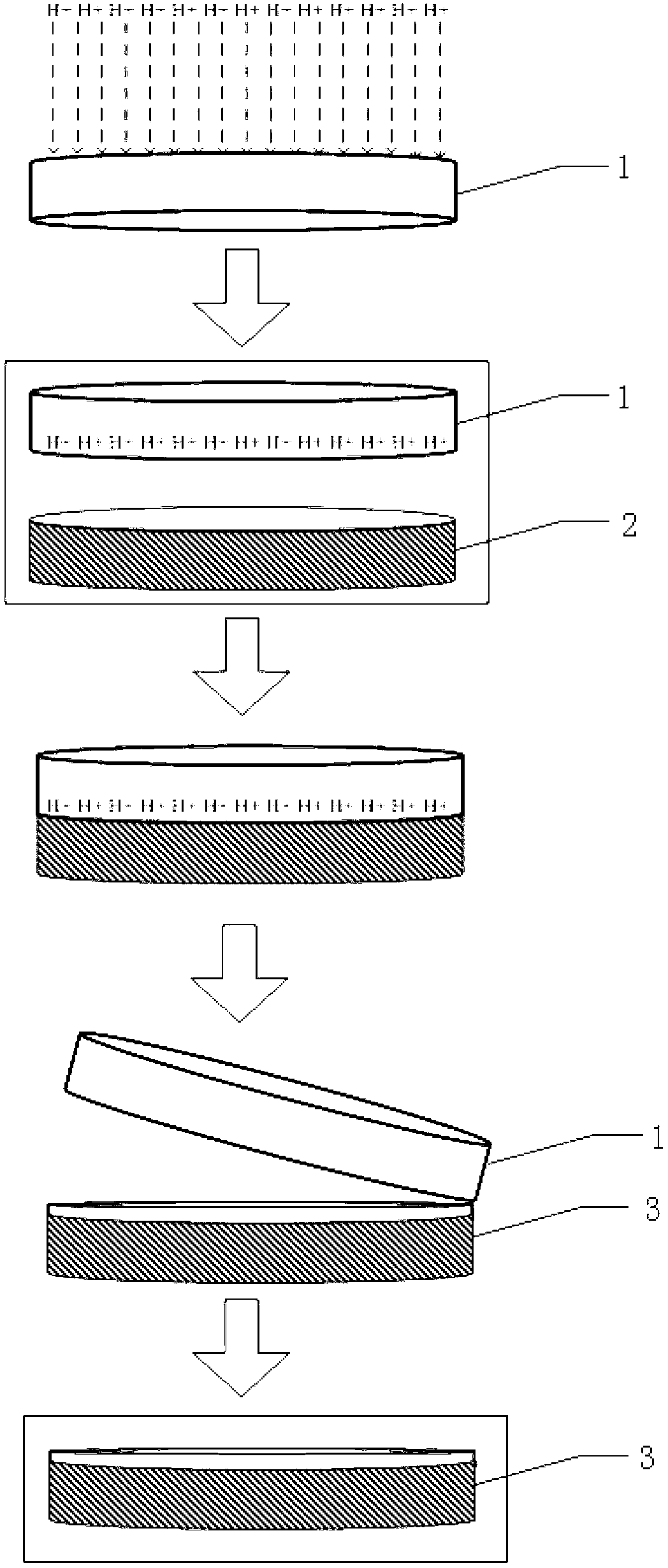
[0035] In this embodiment, the process of preparing a gallium nitride-based semiconductor material epitaxial composite substrate includes the following steps, such as image 3 Shown:

[0036] Step 1: Select an initial SiC wafer 1 and a substrate material 2 . The initial SiC wafer 1 is single crystal SiC with a diameter of 1-6 inches in 4H or 6H phase and a thickness of 0.1-0.8 mm. The substrate material 2 is a single crystal Si or polycrystalline Si wafer with a diameter of 1-6 inches, or a disk made of nitride / oxide ceramic powder sintered, with a thickness of 0.2mm-1mm.

[0037] Step 2: Ion implantation of hydrogen injection intelligent stripping method, the implantation is hydrogen ion, helium ion or co-implantation of both, or B ion and hydrogen ion co-implantation; the implantation energy is 5keV-1000keV, and the implantation dose is 1E15-1E18cm -2 , the implantation temperature is room temperature, and the implanted ions form a bubble layer in the initial SiC wafer 1 ....


PUM

PropertyMeasurementUnit
thicknessaaaaaaaaaa
diameteraaaaaaaaaa
thicknessaaaaaaaaaa

Abstract

The invention discloses a method for preparing an epitaxial composite substrate of a gallium nitride based semiconducting material. The method includes the steps of selecting an initial single crystal silicon carbide wafer and a substrate material; injecting ion in the initial single crystal silicon carbide wafer to form an air bubble layer via a hydrogen-injecting smart-cut method; subjecting the initial single crystal silicon carbide wafer and the substrate material to auxiliary plasma bonding after surface processing including surface cleaning and spin-drying; subjecting the material obtained in the auxiliary plasma bonding to high temperature annealing to enable the air bubble layer of the initial single crystal silicon carbide wafer to converge so as to enable the initial single crystal silicon carbide wafer to jump off, and obtaining a composite single crystal silicon carbide substrate material. By the aid of the method for preparing the epitaxial composite substrate of the gallium nitride based semiconducting material, an epitaxy of the gallium nitride based material is enabled to obtain the high-quality single crystal silicon carbide substrate, and cost for the substrate material can be effectively reduced.

Description

technical field [0001] The invention relates to the preparation technology of semiconductor materials, in particular to a preparation method of a gallium nitride-based semiconductor material epitaxial composite substrate. Background technique [0002] The gallium nitride (GaN)-based quaternary alloy system wide bandgap semiconductor material composed of In-Al-Ga-N has become an important material basis for semiconductor lighting, high-density optical storage, and high-voltage and high-power new semiconductor devices. Semiconductor devices made of GaN-based materials, such as high-brightness blue / white light-emitting diodes (LEDs), blue / violet laser diodes, ultraviolet detectors, high-mobility transistors, high-power transistors, and high-voltage transistors, have been widely used. application. [0003] Because GaN materials cannot obtain bulk-grown single-crystal materials, the preparation of its materials is currently based on epitaxial materials, and the epitaxial substra...

Claims


Application Information

Patent Timeline
Patent Type & Authority Applications(China)
IPC IPC(8): H01L21/02
Inventor 亢勇陈邦明
Owner SHANGHAI XINCHU INTEGRATED CIRCUIT
Why Eureka
Try Eureka