
Light or Gas Detectors Based on Inorganic Semiconductor Single Crystal Network Structure

A technology of inorganic semiconductor and gas detectors, which is applied in photometry and material resistance using electric radiation detectors. It can solve the problems of long response time, small specific surface area, and low resolution of semiconductor sensors, and increase the action position. Points, improved sensitivity, and shortened response time

Active Publication Date: 2016-05-25
SUZHOU JINFU TECH +1
View PDF6 Cites 1 Cited by
  • Summary
  • Abstract
  • Description
  • Claims
  • Application Information

AI Technical Summary

Problems solved by technology

Both structures have their significant disadvantages. The thin-film inorganic semiconductor sensitive element has a small specific surface area, while the polycrystalline network inorganic semiconductor sensitive element has a large specific surface area, but there are more defects.
These reasons lead to low resolution and long response time of semiconductor sensors

Method used


Image

  • Light or Gas Detectors Based on Inorganic Semiconductor Single Crystal Network Structure
  • Light or Gas Detectors Based on Inorganic Semiconductor Single Crystal Network Structure
  • Light or Gas Detectors Based on Inorganic Semiconductor Single Crystal Network Structure

Examples


Embodiment 1

[0025] Step 1, 0.3mmolZnSO 4 ·7H 2 O and 0.3 mmol Na 2 SeO 3 Dissolve in a mixed solution of 16mL deionized water, 14mL diethylenetriamine and 5mL hydrazine hydrate. After magnetic stirring for 30 min, it was transferred to a reaction kettle with a volume of 50 mL, sealed and placed in an oven at 180° C. for 12 h. After natural cooling, the reaction product was washed three times with distilled water and absolute ethanol and dried under vacuum at 60°C.

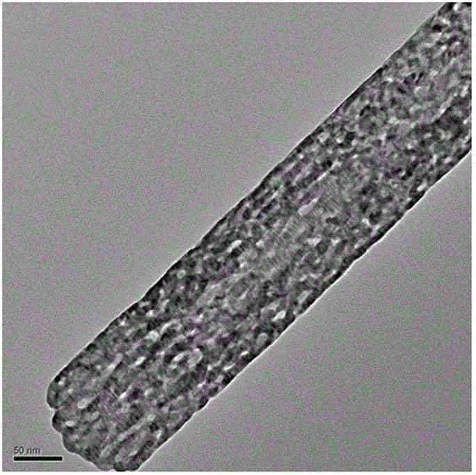
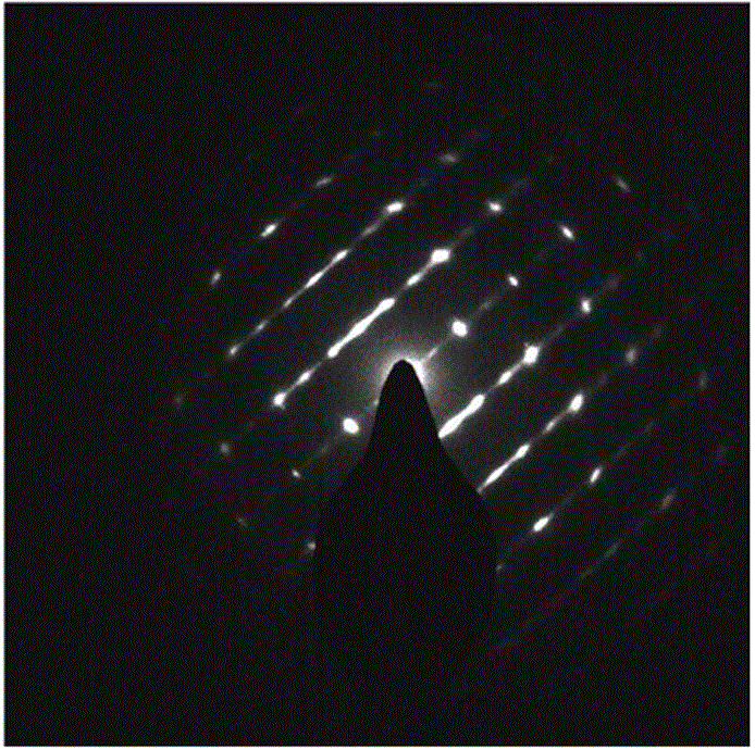
[0026] Step 2, take 0.2mmol of the above product and redisperse it in 35mL of deionized water, and add 0.1mmol of PbCl 2 After stirring for 10 minutes, it was transferred to a 50mL reactor, sealed and placed in an oven at 160°C for 6 hours. After natural cooling, the reaction product was washed three times with distilled water and absolute ethanol to obtain figure 1 Shown Zn 0.5 Pb 0.5 Se network structure nanoribbons. Depend on figure 2 It can be seen that the nanobelt is a single crystal structure.

[0027] Step ...

Embodiment 2

[0030] Step 1, 2.5 mL of 1-hexanol and 0.91 g of cetyltrimethylammonium bromide were dissolved in 25.0 mL of n-dodecane. Then add 1 mL of Zn(AC) with a concentration of 2 mol / L to the above solution 2 ammonia solution and stirred vigorously until the solution was clear and inverse microemulsions formed.

[0031] Step 2, take 50μLCS 2 Dissolve in 2mL of n-dodecane solution, ultrasonically disperse and add dropwise to the above inverse microemulsion system with a syringe. Stirring was continued for about 2 h until the solution turned milky white indicating that ZnS nanoparticles had been generated.

[0032] Step 3: Add 12 mL of diethylene glycol to the milky white solution to break the emulsion, and then let it stand for 3 days. In this process, ZnS nanoparticles self-assembled at the interface of n-dodecane and diethylene glycol through orientation lapping to form Figure 4-5 Porous single crystal microsheets shown.

[0033] Step 4, the ZnS porous single crystal micro-shee...

Embodiment 3

[0036] Step 1: Take a single crystal silicon wafer and use acetone, ethanol, and distilled water to sonicate for 40 minutes, and then use N 2 air-dried and placed in a vacuum oven at 100°C.

[0037] Step 2, mixing nitric acid and hydrofluoric acid in a molar ratio of 4:6 and diluting with distilled water to a dilute acid solution with a mass fraction of 10% is configured as an ink.

[0038] Step 3: inject the ink into the ink tank, etch the cleaned and dried monocrystalline silicon wafer according to a predetermined pattern by conventional inkjet printing technology, and then wash it several times with distilled water to obtain the following: Figure 7 The Si porous monolith shown.

[0039] Step 4, preparing a layer of gold on the Si porous single wafer by thermal evaporation to form the source electrode and the drain electrode.

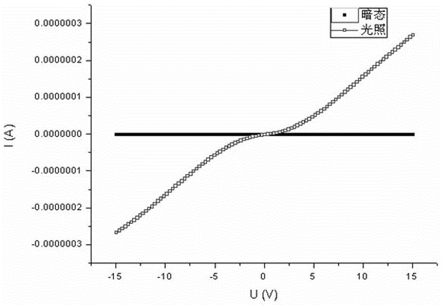
[0040] Step 5, carry out the gas sensitivity detection of oxygen to the above-mentioned sensor, the result is shown in Figure 8 . It can be see...


PUM

PropertyMeasurementUnit
wavelengthaaaaaaaaaa

Abstract

The invention discloses a light or gas detector based on an inorganic semiconductor single crystal network structure. The detector comprises a sensitive element layer, a source electrode and a drainage electrode. The detector is characterized in that: the sensitive element layer is formed by the inorganic semiconductor single crystal network structure. Compared with the sensitive element adopting the film or polycrystal network structure in the traditional detector, the single crystal network structure can enable the semiconductor material as a detecting layer to have a large specific surface area, and the light or gas acting site is increased; and through the single crystal network structure, the number of faults can be obviously reduced, and the electronic transport property is improved. Thus, by the method, the sensitivity of the detector can be obviously improved, the response time is shortened, and the detection efficiency is improved.

Description

technical field [0001] The invention relates to a light or gas detector, in particular to a detector based on an inorganic semiconductor single crystal network structure. Background technique [0002] Semiconductor sensors refer to detection devices that use semiconductor materials as sensitive elements. Among them, the gas sensor is made by using the oxidation and reduction reaction of the gas on the surface of the semiconductor to cause the resistance of the sensitive element to change. When the semiconductor sensitive material contacts the gas, the composition or concentration of the gas to be detected can be detected by measuring the change of the resistance of the semiconductor. Gas sensors are mainly used in the monitoring, forecasting and automatic control of flammable, explosive, toxic and other harmful gases. [0003] Semiconductor photodetectors are devices that use the photoelectric effect of semiconductor materials to receive and detect optical signals. Simila...

Claims


Application Information

Patent Timeline
Patent Type & Authority Patents(China)
IPC IPC(8): G01J1/42G01N27/12
Inventor 张孟李丰潘革波马慧军
Owner SUZHOU JINFU TECH
Learn More