Production method of alloy oxide thin-film transistor

An oxide thin film and transistor technology, which is applied in semiconductor/solid-state device manufacturing, electrical components, circuits, etc., can solve the problems of device integration, reliability and lifespan, leakage current and high power consumption, etc., and achieve excellent deposition uniformity and consistency, improved flatness, and high deposition rate

Inactive Publication Date: 2013-05-22
QINGDAO UNIV
View PDF5 Cites 8 Cited by
  • Summary
  • Abstract
  • Description
  • Claims
  • Application Information

AI Technical Summary

Problems solved by technology

A large leakage current will cause high power consumption and corresponding heat dissipation problems, which will adversely affect the inte

Method used


Image

  • Production method of alloy oxide thin-film transistor
  • Production method of alloy oxide thin-film transistor
  • Production method of alloy oxide thin-film transistor

Examples


Example Embodiment

[0023] Examples:

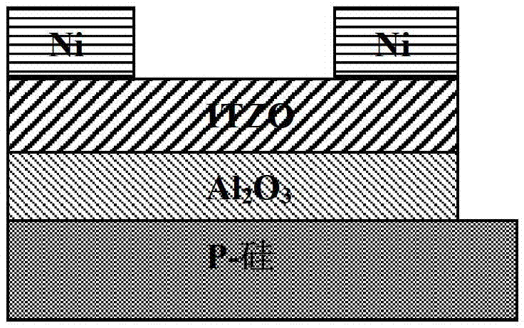
[0024] This embodiment prepares a bottom gate structure based on Al 2 O 3 The specific process of the quaternary alloy oxide thin film transistor is:

[0025] (1) Using laser pulse deposition technology (PLD) to prepare Al 2 O 3 High-k dielectric film:

[0026] Step 1: Choose P-type silicon (100) as the substrate, and wash with acetone with a purity of more than 99% and alcohol with a purity of more than 99% in sequence for 5 minutes by ultrasonic vibration, and then repeatedly rinse with deionized water, and then blow dry with high purity nitrogen;

[0027] Step 2: Put the P-type silicon substrate and alumina ceramic target into the pulsed laser (PLD) reaction chamber, adjust the distance between the alumina ceramic target and the substrate to 40mm, and then extract to high vacuum (10 -5 Pa) After passing in high-purity oxygen, keeping the working pressure of the reaction chamber at 60mTorr, perform pulse laser ablation on the alumina target for 5 minutes, and the l...


PUM

PropertyMeasurementUnit
Thicknessaaaaaaaaaa
Thicknessaaaaaaaaaa
Thicknessaaaaaaaaaa

Abstract

The invention belongs to the technical field of production of semiconductor material thin-film transistors and relates to a production method of an alloy oxide thin-film transistor. After a P-type silicon substrate and an aluminum oxide ceramic target are placed in an existing pulse laser ablation device, the aluminum oxide ceramic target is subjected to pulse laser ablation and an aluminum oxide ceramic target film sample is formed on the P-type substrate by deposition. The surface of the Al2O3 ceramic target film sample is cleaned, ITZO (indium tin zinc oxide) semiconductor channel layer is made on the surface of a gate medium layer of the cleaned Al2O3 ceramic target film sample, TFT (thin film transistor) channels different in length and width are made by photoetching, and alloy semiconductor film channel layer material is deposited on a high-k gate medium layer at room temperature by radio frequency magnetron sputtering technology. Ni is deposited at room temperature by ion beam sputtering technology to form a source electrode and a drain electrode. The source electrode and the drain electrode are obtained after photoresist is stripped, and the alloy oxide thin-film transistor is obtained after annealing. The production process is simple, the principle is reliable, production performance is fine, production is environment-friendly, and the production method is low in cost and widely applicable.

Description

Technical field: [0001] The invention belongs to the technical field of semiconductor material thin film transistor preparation, and relates to a high-k dielectric aluminum oxide (Al 2 o 3 ) and the preparation process of a new semiconductor channel material indium titanium zinc oxide (In-Ti-Zn-O, ITZO) quaternary alloy oxide thin film transistor, especially a preparation method of an alloy oxide thin film transistor. Background technique: [0002] In recent years, thin-film transistors (ThinFilm Transistor, TFT) have played an important role in Active Matrix Liquid Crystal Display (AMLCD), from low-temperature amorphous silicon TFT to high-temperature polysilicon TFT, the technology has become more and more mature, and the application The object has developed from only driving LCD (LiquidCrystal Display) to both driving LCD and OLED (OrganicLight Emitting Display) and electronic paper. With the continuous improvement of the semiconductor process level, the pixel size is c...

Claims


Application Information

Patent Timeline
IPC IPC(8): H01L21/336H01L21/285H01L21/203
Inventor 单福凯刘奥刘国侠朱慧慧
Owner QINGDAO UNIV
Why Eureka
Try Eureka