Ambipolar inverter device structure and manufacturing method thereof

A technology of component structure and manufacturing method, applied in the field of dual carrier inverter component structure and its manufacturing, can solve the problems of material property damage, occupation area, complex process and the like

Inactive Publication Date: 2013-06-19
IND TECH RES INST
View PDF4 Cites 2 Cited by
  • Summary
  • Abstract
  • Description
  • Claims
  • Application Information

AI Technical Summary

Problems solved by technology

However, how to fabricate the N-type and P-type active layers on the same substrate at the same time requires a separate patterning process, which is quite difficult to avoid damage to the material properties of each layer
[0005] In the above two methods, whether it is two single-polarity transistors or two different-polarity transistors to form a CMOS inverter, two components are required to be combined, which takes up a lot of area and the process is relatively simple. complex

Method used


Image

  • Ambipolar inverter device structure and manufacturing method thereof
  • Ambipolar inverter device structure and manufacturing method thereof
  • Ambipolar inverter device structure and manufacturing method thereof

Examples


no. 1 example

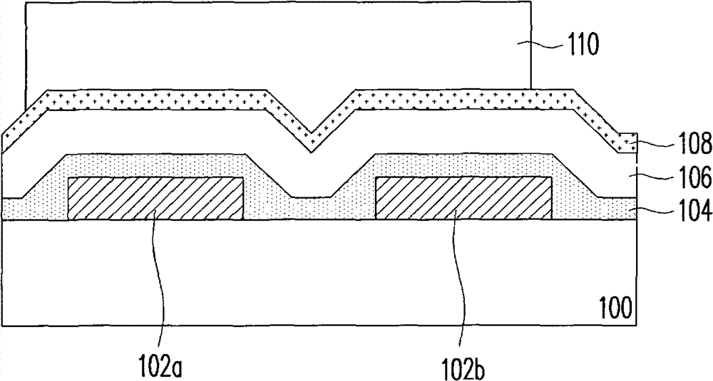
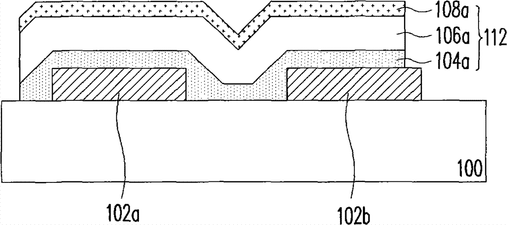
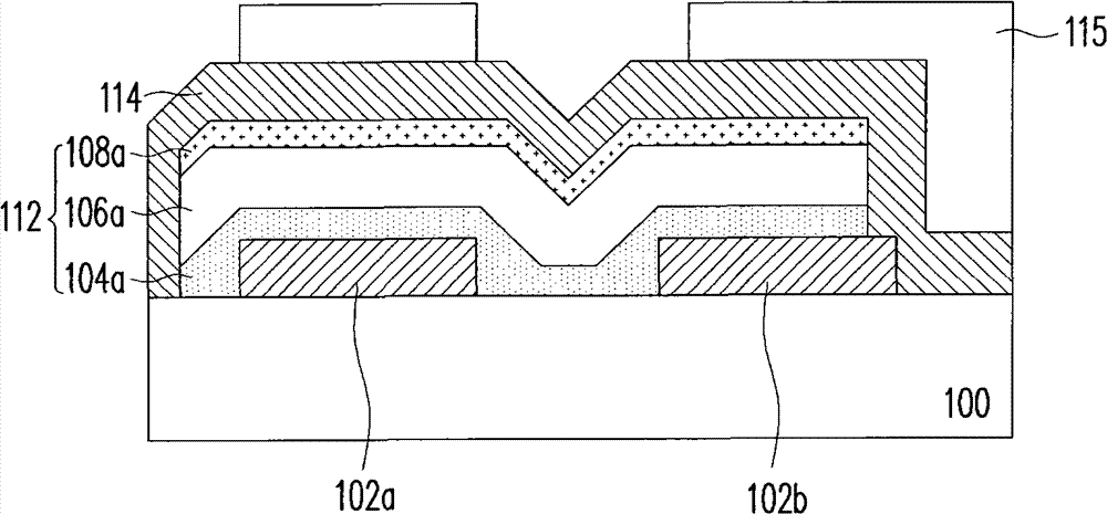
[0106] Figure 1A-1D It is a schematic cross-sectional view of the manufacturing method of the bicarrier inverter assembly structure according to the first embodiment of the present invention.

[0107] Please refer to Figure 1A , forming an electrode 102 a and an electrode 102 b separated from each other on the substrate 100 . The substrate 100 can be a rigid substrate or a flexible substrate. Materials for rigid substrates are, for example, glass, quartz or silicon wafers. The material of the flexible substrate is, for example, plastic such as acrylic, metal foil or paper. The electrode 102 a and the electrode 102 b are formed by, for example, first forming an electrode layer (not shown) on the substrate 100 , and then patterning the electrode layer by using lithography and etching processes. The material of the electrode layer is, for example, gold, silver, copper, aluminum, molybdenum, chromium, etc. or alloys thereof. The method for forming the electrode layer include...

no. 2 example

[0125] Figure 2A-2B It is a schematic cross-sectional view of the manufacturing method of the bicarrier inverter assembly structure according to the second embodiment of the present invention. The bipolar inverter assembly structure 20 of the second embodiment is similar to the bipolar inverter assembly structure 10 of the first embodiment, the differences will be described below, and the similarities will not be repeated.

[0126] First, please refer to Figure 2A , forming a gate 202 on the substrate 200 . Then, a dielectric layer 204 covering the gate 202 is formed on the substrate 200 . Next, an electrode 206 a and an electrode 206 b are formed on the dielectric layer 204 . Materials and formation methods of the gate 202, dielectric layer 204, electrode 206a, and electrode 206b of the second embodiment are similar to those of the gate 118, dielectric layer 116, electrode 102a, and electrode 102b of the first embodiment, and are not repeated here. repeat.

[0127] Aft...

example 1

[0137] The substrate is a P-type silicon wafer (30-60Ω-cm, crystal plane). Then, 200nm of silicon oxide is formed on the substrate as a dielectric layer. Then, two silver electrodes are formed on the dielectric layer. Then, on the dielectric layer and the silver electrode, vapor-deposit as electron blocking layer m-MTDATA thin film. Afterwards, the substrate was placed in a vacuum chamber and evacuated to 2.5×10 -6 torr, using a boron nitride crucible (BN crucible) to The plating rate of PTCDI-C13 as an N-type organic semiconductor material and pentacene (pentacene) as a P-type organic semiconductor material were vapor-deposited respectively to form a bipolar semiconductor layer. At this time, the film thickness is monitored by a quartz oscillator, and then calibrated by a white light interferometer to form The PTCDI-C13 film and pentacene film. Then, on the bipolar semiconductor layer, vapor-deposit as electron blocking layer m-MTDATA thin film. Note that the s...


PUM


Abstract

An ambipolar inverter device suitable for use in an integrated circuit. An electron blocking layer and a hole blocking layer are respectively disposed at two sides of the ambipolar semiconductor layer, so that the operation of the inverter may be executed in a single device. In addition, the manufacturing method of the disclosure is simple, adopting only one patterning step, so as to effectively improve the performance of the ambipolar device.

Description

technical field [0001] The invention relates to a semiconductor component and its manufacturing method, in particular to a bicarrier inverter component structure and its manufacturing method. Background technique [0002] An inverter is a basic component in an integrated circuit. The inverter can invert the phase of the input signal by 180 degrees. This circuit is used in analog circuits, such as audio amplifiers, clock oscillators, etc. In the design of electronic circuits, inverters are often used. [0003] In general, there are two ways to make an inverter. The first is to make a unipolar inverter, which directly consists of two unipolar transistors (PMOS or NMOS) to form complementary logic. Since it is directly constructed of a single-type PMOS or NMOS, only one type of metal is required for the source / drain electrodes, and only a single-type (P-type or N-type) material is required for the active layer material, so the advantage is that it can be simplified Technolo...

Claims


Application Information

Patent Timeline
Patent Type & Authority Applications(China)
IPC IPC(8): H01L27/02H01L21/822
CPCH10K19/10H10K85/621H10K85/324H10K10/486
Inventor 宋兆峰谢彦敏
Owner IND TECH RES INST
Why Eureka
Try Eureka