Copper plating solution for PCB (printed circuit board) blind holes, as well as preparation method and plating method of copper plating solution
A technology of electroplating copper and solution, which is applied in the direction of electrical connection formation of printed components, etc., and can solve problems such as ductility, poor gloss and toughness, uneven copper plating layer, and low hole filling rate
- Summary
- Abstract
- Description
- Claims
- Application Information
AI Technical Summary
Problems solved by technology
Method used
Image

Examples
Embodiment 1
[0089] A kind of electroplating copper solution for PCB blind hole, each component and content thereof of described copper electroplating solution are:
[0090] Copper sulfate pentahydrate: 100g / L
[0091] Sulfuric acid: 50g / L
[0093] Brightener: 5g / L
[0094] Carrier: 3g / L
[0095] Leveling agent: 2g / L
[0096] Deionized water balance;
[0097] And the concentration ratio of copper sulfate pentahydrate to sulfuric acid is 2:1.
[0098] The brightener is a mixture of sodium polydithiodipropane sulfonate and ethylene thiourea with a weight ratio of 1.5:1; the carrier is polypropylene glycol with a molecular weight of 500.
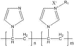
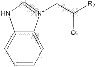
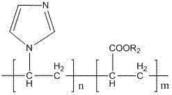
[0099] The leveling agent is a mixture of leveling agent A and leveling agent B with a weight ratio of 1.2:1; wherein, the leveling agent A is a polyvinylimidazolium quaternary ammonium compound, and the leveling agent B is N- Vinylimidazole-ethyl acrylate copolymer.
[0100] The structural formula of the leveling agent ...
Embodiment 2
[0118] A kind of electroplating copper solution for PCB blind hole, each component and content thereof of described copper electroplating solution are:
[0119] Copper sulfate pentahydrate: 150g / L
[0120] Sulfuric acid: 80g / L
[0122] Brightener: 15g / L
[0123] Carrier: 10g / L
[0124] Leveling agent: 5g / L
[0125] Deionized water balance;
[0126] And the concentration ratio of copper sulfate pentahydrate to sulfuric acid is 1.88:1.
[0127] The brightener is a mixture of sodium polydithiodipropane sulfonate and ethylene thiourea with a weight ratio of 2:1; the carrier is polypropylene glycol with a molecular weight of 800.
[0128] The leveling agent is a mixture of leveling agent A and leveling agent B with a weight ratio of 1.5:1; wherein, the leveling agent A is a polyvinylimidazolium quaternary ammonium compound, and the leveling agent B is N- Vinylimidazole-ethyl acrylate copolymer.
[0129] The structural formula of the leveling age...
Embodiment 3
[0147] A kind of electroplating copper solution for PCB blind hole, each component and content thereof of described copper electroplating solution are:
[0148] Copper sulfate pentahydrate: 200g / L
[0149] Sulfuric acid: 120g / L
[0151] Brightener: 25g / L
[0152] Carrier: 15g / L
[0153] Leveling agent: 10g / L
[0154] Deionized water balance;
[0155] And the concentration ratio of copper sulfate pentahydrate to sulfuric acid is 1.67:1.
[0156] The brightener is a mixture of sodium polydithiodipropane sulfonate and ethylene thiourea with a weight ratio of 2.5:1; the carrier is polypropylene glycol with a molecular weight of 1000.
[0157] The leveling agent is a mixture of leveling agent A and leveling agent B with a weight ratio of 1.8:1; wherein, the leveling agent A is a polyvinylimidazolium quaternary ammonium compound, and the leveling agent B is N- Vinylimidazole-ethyl acrylate copolymer.
[0158] The structural formula of the levelin...
PUM
 Abstract
Description
Claims
Application Information
 - R&D
- Intellectual Property
- Life Sciences
- Materials
- Tech Scout
- Unparalleled Data Quality
- Higher Quality Content
- 60% Fewer Hallucinations
Browse by: Latest US Patents, China's latest patents, Technical Efficacy Thesaurus, Application Domain, Technology Topic, Popular Technical Reports.
© 2025 PatSnap. All rights reserved.Legal|Privacy policy|Modern Slavery Act Transparency Statement|Sitemap|About US| Contact US: help@patsnap.com