Thin-film solar cell with micron-nanometer two-stage array structure and manufacturing method thereof

A technology of solar cells and array structures, applied in the fields of nanotechnology, nanotechnology, nanotechnology for materials and surface science, etc., can solve the problems of high cost and low conversion rate of solar cells, and reduce the preparation cost and equipment requirements. The effect is not high and the preparation method is simple

Active Publication Date: 2014-04-09
SHANGQIU NORMAL UNIVERSITY
View PDF4 Cites 6 Cited by
  • Summary
  • Abstract
  • Description
  • Claims
  • Application Information

AI Technical Summary

Problems solved by technology

[0010] In view of the above situation, in order to overcome the defects of the prior art, the object of the present invention is to provide a kind of micro / nano secondary array structure thin film solar cell and its preparation method, It can effectively solve the problems of low conversion rate and high cost of solar cells

Method used


Image

  • Thin-film solar cell with micron-nanometer two-stage array structure and manufacturing method thereof

Examples


Embodiment 1

[0032] The preparation method of the micro / nano secondary array structure thin-film solar cell of this embodiment comprises the following steps:

[0033] (1) Polish the copper sheet with sandpaper No. 0-6, and ultrasonically clean it with alcohol, acetone, and deionized water for 5 minutes; then magnetron sputtering a layer of Mo on the copper sheet, and the thickness of Mo is 800nm;

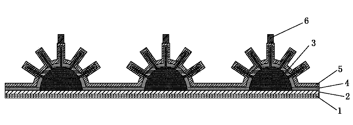
[0034] (2) Pulse electrochemical deposition of a copper film with a thickness of 1 μm on the copper sheet deposited with the Mo layer; then put the copper sheet deposited with the copper film into the oxygen / hydrogen sulfide mixed gas, the volume ratio of oxygen and hydrogen sulfide 1:2, put it at 11°C for 16h, so that the copper film becomes Cu 2 S Micro / Nano Secondary Array, Cu 2 S nanowires have a diameter of 50nm and a length of 10μm; Cu 2 The diameter of the S spherical cap is 8 μm, Cu 2 The interval between the S spherical caps is 2 μm; then the treated copper sheet is placed in an aque...

Embodiment 2

[0041] The preparation method of the micro / nano secondary array structure thin-film solar cell of this embodiment comprises the following steps:

[0042] (1) The glass sheet was ultrasonically cleaned with 1mol / L NaOH, 1mol / L HCl solution, absolute ethanol, and deionized water in sequence, and then a layer of ITO was magnetron sputtered on the glass sheet, and the thickness of ITO was 200nm;

[0043] (2) Electrochemically deposit a layer of copper film with a thickness of 500nm on the glass sheet deposited with ITO at constant voltage; put the glass sheet deposited with copper film into the oxygen / hydrogen sulfide mixed gas, the volume ratio of oxygen and hydrogen sulfide is 1:100, put it at 0°C for 500h to make the copper film into Cu 2 S Micro / Nano Secondary Array, Cu 2 S nanowires have a diameter of 10nm and a length of 100nm; Cu 2 The diameter of the S spherical cap is 100 μm, Cu 2 The interval between the S spherical caps is 50 μm; then place the treated glass sheet in...

Embodiment 3

[0050] The preparation method of the micro / nano secondary array structure thin-film solar cell of this embodiment comprises the following steps:

[0051] (1) Electron beam evaporation of a layer of Mo on the newly cut mica sheet, the thickness of Mo is 800nm;

[0052] (2) A copper film with a thickness of 1 μm was electrochemically deposited on the mica sheet deposited with Mo at a constant current; the mica sheet deposited with the copper film was placed in a mixed gas of oxygen / hydrogen sulfide, and the volume ratio of oxygen and hydrogen sulfide was 1:0.01, put it at 200°C for 12 hours to make the copper film into Cu 2 S Micro / Nano Secondary Array, Cu 2 S nanowires have a diameter of 500nm and a length of 300μm; Cu 2 The diameter of the S spherical cap is 0.5μm, Cu 2 The interval between the S spherical caps is 100 μm; then the treated mica sheet is placed in an aqueous hydrochloric acid solution with a concentration of 0.01mol / L to dissolve the oxide layer generated on ...


PUM


Abstract

The invention belongs to the technical field of solar photovoltaic cells, and particularly relates to a thin-film solar cell with a micron-nanometer two-stage array structure and a manufacturing method of the thin-film solar cell. The thin-film solar cell comprises a substrate, wherein a back electrode, a p-type semiconductor micron-nanometer two-stage array, an n-type semiconductor layer, a window layer and a metal grid electrode are sequentially arranged on the substrate. An absorbing layer of the thin-film solar cell with the micron-nanometer two-stage array structure is manufactured on the basis of a Cu2S micron-nanometer two-stage array through the chemical bath deposition technology, and the manufacturing method is simple; compared with a method that high vacuum conditions or high temperature conditions are needed for manufacturing the absorbing layer, the manufacturing method has the advantages that the cost is low, the requirements for equipment are low, reactants are easy to obtain, the preparation temperature is low, reaction conditions are easy to control, and the manufacturing method can be conveniently and widely applied.

Description

technical field [0001] The invention belongs to the technical field of solar photovoltaic cells, in particular to a thin-film solar cell with a micron / nano secondary array structure and a preparation method thereof. Background technique [0002] Solar cells are one of the effective ways for human beings to utilize solar energy. At present, the solar cell materials that have been studied more include monocrystalline silicon, polycrystalline silicon, amorphous silicon, gallium arsenide, cadmium sulfide, cadmium tellurium, copper indium sulfur, copper indium gallium selenide, copper indium gallium selenide sulfur, etc. Among them, copper indium gallium selenide (CIGS) solar cell material is a new generation of more promising materials. CIGS is a direct bandgap semiconductor, which has the advantages of high light absorption coefficient, high photoelectric conversion efficiency, long life, good weak light performance, and strong radiation resistance. The photoelectric conversi...

Claims


Application Information

Patent Timeline
Patent Type & Authority Applications(China)
IPC IPC(8): H01L31/0236H01L31/18
CPCY02E10/50B82Y30/00B82Y40/00H01L31/02363H01L31/032H01L31/18Y02P70/50
Inventor 李立强任山陈文聪陈圆圆
Owner SHANGQIU NORMAL UNIVERSITY
Why Eureka
Try Eureka