Purple LED (light-emitting diode) preparation method, purple LED and chip

A purple light and crystal nucleus technology, which is applied in the direction of electrical components, circuits, semiconductor devices, etc., can solve the problems of purple light LEDs such as poor antistatic performance, easy to generate dislocations, and poor luminous efficiency

Active Publication Date: 2014-04-23
EPITOP PHOTOELECTRIC TECH
View PDF5 Cites 5 Cited by
  • Summary
  • Abstract
  • Description
  • Claims
  • Application Information

AI Technical Summary

Problems solved by technology

[0003] However, the traditional blue LED uses gallium nitride as the barrier layer of the quantum well, and indium gallium nitrogen as the well layer of the quantum well, but the short-wavelength violet LED is determined by the material characteristics of the well layer, that is, the light-emitting layer. If the traditional LED structure is still used Gallium nitride is used as a barrier layer, the band gap width between materials is relatively small and the barrier height is low, the abilit

Method used


Image

  • Purple LED (light-emitting diode) preparation method, purple LED and chip
  • Purple LED (light-emitting diode) preparation method, purple LED and chip
  • Purple LED (light-emitting diode) preparation method, purple LED and chip

Examples


Embodiment 1

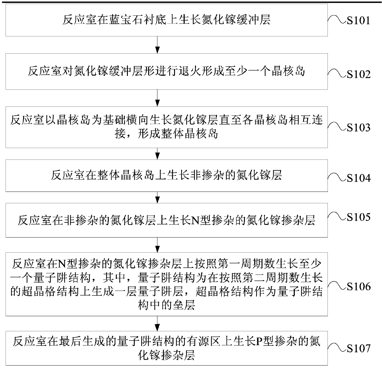
[0023] figure 1 The flow chart of the preparation method of purple light LED provided by the present invention, such as figure 1 As shown, the method includes:

[0024] It should be noted that this method can be implemented in growth equipment, which can be metal-organic chemical vapor deposition equipment (Metal-organic Chemical Vapor Deposition, MOCVD), molecular beam epitaxy equipment (Molecular Beam Epitaxy, MBE) or hydride vapor phase epitaxy equipment (Hydride Vapor Phase Epitaxy, HVPE).

[0025] S101. A reaction chamber grows a gallium nitride buffer layer on a sapphire substrate.

[0026] For example, when the temperature is 530°C and the pressure is 500torr, the reaction chamber is fed with trimethylgallium and NH3 for about 3.5 minutes at the same time, and at least one gallium nitride GaN buffer layer with a thickness of 5nm-60nm is grown on the sapphire substrate , wherein the feed rate of trimethylgallium is 150ml / min. Preferably, the thickness of the grown ga...

Embodiment 2

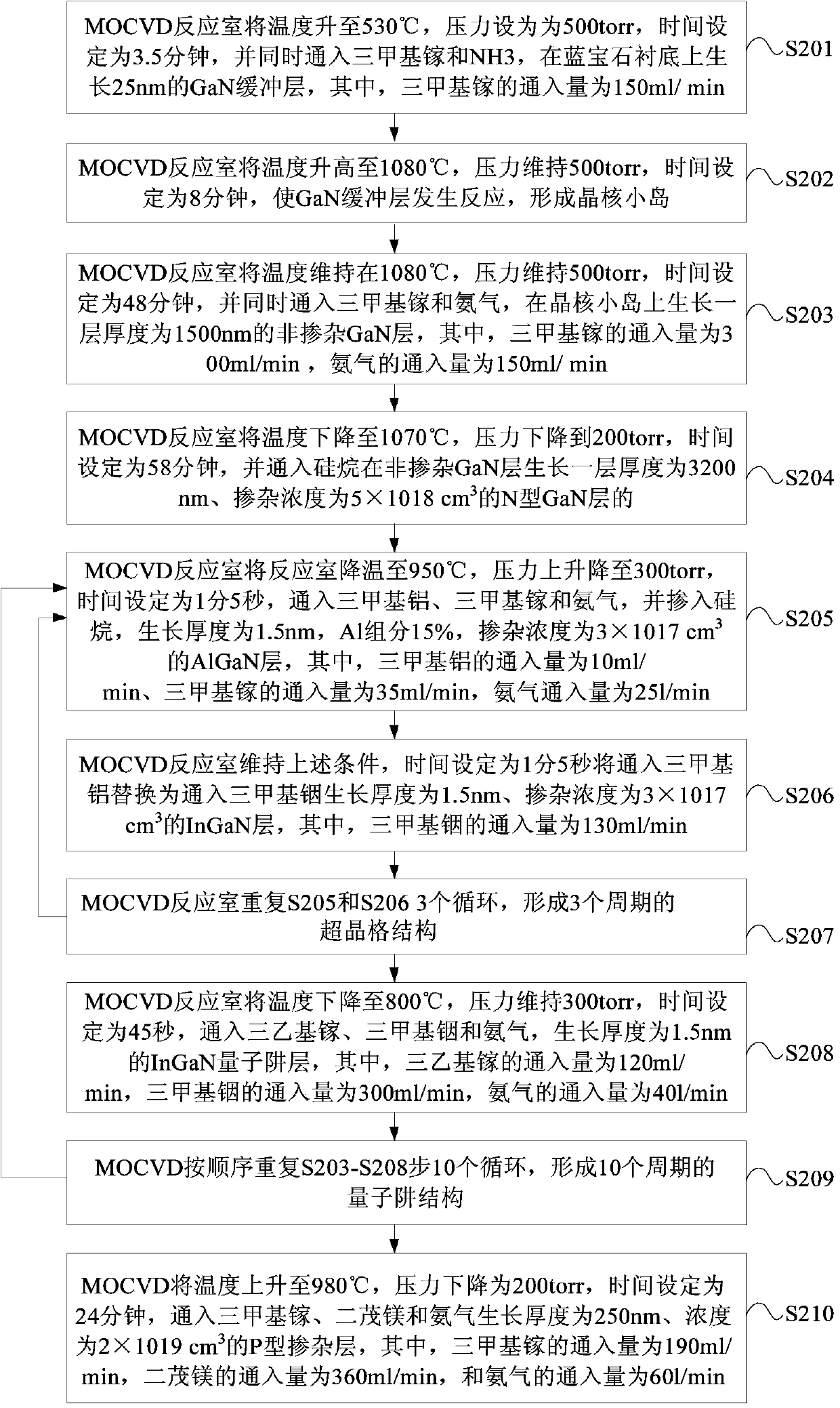
[0046] figure 2 The flowchart of another preparation method for purple LED provided by the present invention is illustrated by taking MOCVD reaction chamber such as purple LED with a growth wavelength of 390nm as an example, as figure 2 As shown, the method includes:

[0047] S201. The temperature of the MOCVD reaction chamber is raised to 530° C., the pressure is set to 500 torr, and the time is set to 3.5 minutes, and trimethylgallium and NH3 are simultaneously introduced to grow a 25 nm GaN buffer layer on the sapphire substrate, wherein, The feed rate of trimethylgallium is 150ml / min.

[0048] S202. The temperature of the MOCVD reaction chamber is raised to 1080° C., the pressure is maintained at 500 torr, and the time is set at 8 minutes, so that the GaN buffer layer reacts to form crystal nucleus islands.

[0049] S203. The MOCVD reaction chamber maintains the temperature at 1080°C, the pressure at 500 torr, the time is set at 48 minutes, and trimethylgallium and amm...

Embodiment 3

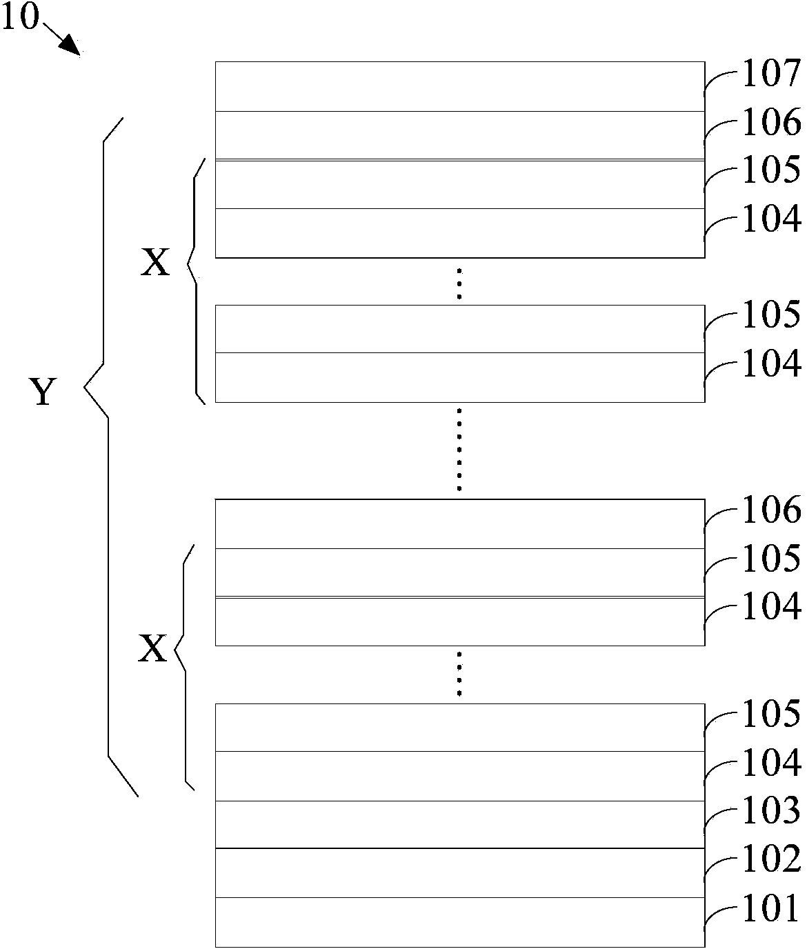
[0059] image 3 The structural representation of the purple LED provided by the present invention, such as image 3 As shown, the violet LED10 includes:

[0060] GaN buffer layer 101, undoped GaN cladding layer 102, N-type doped layer 103, AlGaN layer 104 in the superlattice, InGaN 105 in the superlattice, InGaN quantum well layer 106, P-type electron blocking layer 107 and P-type doped layer 108, and, image 3 The X in it is 2-20, and the Y is 2-20.

[0061] Further, the AlGaN layer 104 in the superlattice and the InGaN 105 in the superlattice constitute a superlattice structure as a quantum barrier layer in the quantum well structure.

[0062] It should be noted that the purple LED 10 can be based on the above-mentioned embodiments and figure 1 with figure 2 Prepared by the method shown, the structure is as image 3 shown.

[0063] The preparation method of the violet LED provided by the embodiment of the present invention includes: growing a gallium nitride buffer l...


PUM

PropertyMeasurementUnit
Thicknessaaaaaaaaaa
Thicknessaaaaaaaaaa
Thicknessaaaaaaaaaa

Abstract

The embodiment of the invention provides a purple LED (light-emitting diode) preparation method, a purple LED and a chip. The method comprises the following steps of growing a gallium nitride buffer layer on a sapphire substrate; annealing the gallium nitride buffer layer to form at least one crystal nucleus island; transversely growing a gallium nitride layer based on the crystal nucleus islands until the crystal nucleus islands are connected with one another to form an integrated crystal nucleus island; growing an undoped gallium nitride layer on the integrated crystal nucleus island; growing an N-type doped gallium nitride layer on the undoped gallium nitride layer; growing at least one quantum well structure on the N-type doped gallium nitride layer according to a first cycle number, wherein each quantum well structure is formed by generating a quantum well layer on a superlattice structure grown according to a second cycle number, and the superlattice structures are used as barrier layers of the quantum well structures; growing a P-type doped gallium nitride layer on an active area of a finally generated quantum well structure. According to the purple LED preparation method, the purple LED and the chip, the charge-carrier recombination probability, the luminous efficiency and the antistatic performance of the purple LED can be improved.

Description

technical field [0001] Embodiments of the present invention relate to the field of semiconductor light-emitting diodes (Light-Emitting Diode, LED), and in particular to a method for preparing a violet LED, a violet LED and a chip. Background technique [0002] LED has the characteristics of high luminous efficiency, long life, small size, and rich colors, and is widely used, especially the wide application of short-wavelength LED in environmental protection, medical equipment, bioengineering and other fields makes it develop rapidly. LEDs emit light by radiative recombination of electrons and holes in the active region sandwiched between the N-type doped region and the P-type doped region. In order to increase the recombination probability of electrons and holes and improve brightness, the traditional LED active area adopts a quantum well structure. In the luminescent layer, recombination is carried out, thereby increasing the probability of radiative recombination. General...

Claims


Application Information

Patent Timeline
IPC IPC(8): H01L33/06H01L33/00
CPCH01L33/0066H01L33/0075H01L33/06
Inventor 于浩郑远志周德保杨东陈向东康建梁旭东
Owner EPITOP PHOTOELECTRIC TECH
Why Eureka
Try Eureka