Gallium oxide heterogeneous structure as well as growth method and special device thereof

A growth method and a heterojunction technology are applied to the nanoscale gallium oxide heterojunction structure, the gallium oxide heterojunction structure and the growth field thereof, and can solve the problems of difficulty in obtaining the heterojunction structure, cumbersome nano-gallium oxide materials, and the like, Achieve the effect of uniform size, huge specific surface area and high growth yield

Active Publication Date: 2014-07-16
INST OF METAL RESEARCH - CHINESE ACAD OF SCI
View PDF0 Cites 16 Cited by
  • Summary
  • Abstract
  • Description
  • Claims
  • Application Information

AI Technical Summary

Problems solved by technology

[0005] The purpose of the present invention is to provide a novel gallium oxide heterojunction structure and its preparation method and special device, to solve the problems in the prior art that the preparation of nano-gallium oxide materials is relatively cumbersome, and it is difficult to obtain a heterojunction structure.

Method used


Image

  • Gallium oxide heterogeneous structure as well as growth method and special device thereof
  • Gallium oxide heterogeneous structure as well as growth method and special device thereof
  • Gallium oxide heterogeneous structure as well as growth method and special device thereof

Examples


Embodiment 1

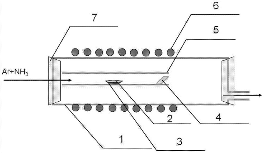
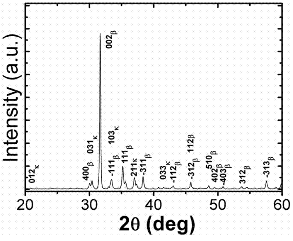
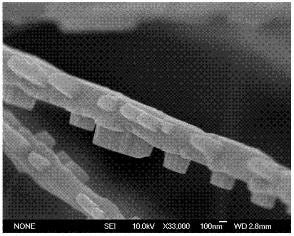
[0044] This embodiment is directly deposited and grown k-Ga on the surface of Si sheet2 o 3 / β-Ga 2 o 3 The heterojunction structure is as follows:

[0045] 1. Weigh a certain mass of β-Ga 2 o 3 Powder, filled with 1 / 2 volume of β-Ga in alumina ceramic boat 2 o 3 Powder, used β-Ga 2 o 3 The purity is 99.99wt%; then the alumina ceramic boat is placed in the center of the quartz tube, and a silicon wafer is placed 25-35 cm downstream of the quartz tube as a substrate for the deposition and growth of gallium oxide nanostructures. In this example, the silicon wafer used has a purity of >99.99wt%, a surface crystal orientation of , single-sided grinding, a surface roughness (Ra)≦0.3nm, a surface size of 20×20mm, and a thickness of 0.5mm.

[0046] 2. Use a mechanical pump to pump the air pressure in the quartz tube to 10 -2 Pa, into the quartz tube in step 1 with a flow rate of 200 sccm of argon for 30 minutes to normal pressure, get rid of residual gas in the quartz tube, ...

Embodiment 2

[0058] The difference from Example 1 is that this example directly deposits and grows k-Ga on the surface of Si sheet 2 o 3 / β-Ga 2 o 3 The heterojunction structure is as follows:

[0059] 1. Weigh a certain mass of β-Ga 2 o 3 Powder, filled with 1 / 2 volume of β-Ga in alumina ceramic boat 2 o 3 Powder, used β-Ga 2 o 3 The purity is 99.99wt%; then the alumina ceramic boat is placed in the center of the quartz tube, and a silicon wafer is placed 25-30 cm downstream of the quartz tube as a substrate for the deposition and growth of gallium oxide nanostructures. In this example, the silicon wafer used has a purity of >99.99wt%, a surface crystal orientation of , single-sided grinding, a surface roughness (Ra)≦0.3nm, a surface size of 20×20mm, and a thickness of 0.5mm.

[0060] 2. Use a mechanical pump to pump the air pressure in the quartz tube to 10 -3 P a , into the quartz tube in step 1 with a flow rate of 100 sccm of argon for 40 minutes to normal pressure, to remov...

Embodiment 3

[0070] The difference from Example 1 is that this example directly deposits and grows k-Ga on the surface of Si sheet 2 o 3 / β-Ga 2 o 3 The heterojunction structure is as follows:

[0071] 1. Weigh a certain mass of β-Ga 2 o 3 Powder, filled with 1 / 2 volume of β-Ga in alumina ceramic boat 2 o 3 Powder, used β-Ga 2 o3 The purity is 99.99wt%; then the alumina ceramic boat is placed in the center of the quartz tube, and a silicon wafer is placed 30-35 cm downstream of the quartz tube as a substrate for the deposition and growth of gallium oxide nanostructures. In this example, the silicon wafer used has a purity of >99.99wt%, a surface crystal orientation of , single-sided grinding, a surface roughness (Ra)≦0.3nm, a surface size of 20×20mm, and a thickness of 0.5mm.

[0072] 2. Use a mechanical pump to pump the air pressure in the quartz tube to 10 -1 P a , into the quartz tube in step 1 with a flow rate of 150 sccm of argon for 30 minutes to normal pressure to remove r...


PUM

PropertyMeasurementUnit
diameteraaaaaaaaaa
heightaaaaaaaaaa
lengthaaaaaaaaaa

Abstract

The invention belongs to the technical field of semiconductor materials and nanometer, specifically relates to a gallium oxide heterogeneous structure and a growth method thereof, and particularly relates to a method and a special device for a gallium oxide heterogeneous structure with a pseudo quartic symmetry nanometer size formed by beta-Ga2O3 and k-Ga2O3. The gallium oxide heterojunction comprises a beta-Ga2O3 nanowire trunk and a k-Ga2O3 nanorod on the surface of the beta-Ga2O3 nanometer linear trunk, wherein the length of the beta-Ga2O3 nanowire is 5-100 mu m and the diameter is 50-1000nm; the size of the k-Ga2O3 nanorod is 50-200nm and is distributed on the nanowire surface in a mode of pseudo quartic symmetry. The method adopted in the invention can be used for accurately controlling the temperature and ammonia gas flow in a deposition area in the process of chemical vapor deposition (CVD), so as to spontaneously form a k-Ga2O3 / beta-Ga2O3 heterogeneous structure, and the obtained k-Ga2O3 is a new crystal structure in a gallium oxide system and has rhombic symmetry. The prepared k-Ga2O3 / beta-Ga2O3 heterogeneous structure has extremely strong cathode ray fluorescence property in an ultraviolet region, has the discrete characteristic of luminescence and is suitable for serving as an ultraviolet light electricity detector and suitable for hydrogen production through photocatalytic water splitting.

Description

technical field [0001] The invention belongs to the field of semiconductor materials and nanotechnology, in particular to a gallium oxide heterojunction structure and a growth method thereof, in particular to a β-Ga 2 o 3 and k-Ga 2 o 3 Methods and dedicated devices for forming nanoscale gallium oxide heterojunction structures with pseudo-quartic symmetry. Background technique [0002] As a typical wide-bandgap oxide semiconductor material, gallium oxide has wide application potential in the field of optoelectronic devices, and can be used to prepare field effect transistors, transparent conductive electrodes, high-temperature gas-phase sensors, and photodetectors. Due to the small size and large specific surface area of ​​nanoscale gallium oxide materials, they exhibit different physical and chemical properties from bulk gallium oxide materials. On the other hand, gallium oxide has a variety of crystal forms, and different crystal forms have different structural stabili...

Claims


Application Information

Patent Timeline
Patent Type & Authority Applications(China)
IPC IPC(8): C30B29/16C30B25/00C30B29/62B82Y30/00B82Y40/00
Inventor 姜辛杨兵刘宝丹
Owner INST OF METAL RESEARCH - CHINESE ACAD OF SCI
Why Eureka
Try Eureka