

LED transparent conductive layer roughening method and vacuum apparatus
A transparent conductive layer and roughness technology, applied in chemical instruments and methods, circuits, electrical components, etc., can solve problems such as complex process, increase LED forward voltage, damage device performance, etc., achieve obvious roughening effect and improve light output efficiency, reducing the effect of total reflection
- Summary
- Abstract
- Description
- Claims
- Application Information
AI Technical Summary
Problems solved by technology
Method used
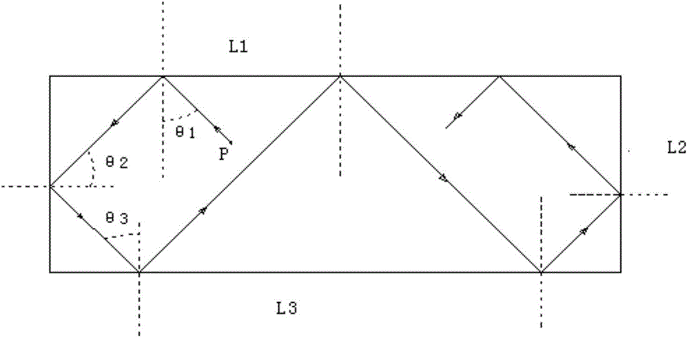
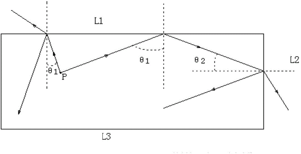
Image

Examples
Embodiment 1
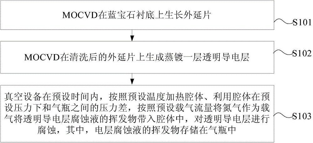
[0023] figure 2 The schematic flow sheet of the roughening method of LED transparent conductive layer provided by the present invention, as figure 2 As shown, the method includes:
[0024] It should be noted that metal-organic chemical vapor deposition equipment (Metal-organic Chemical Vapor Deposition, MOCVD) can be used to grow epitaxial wafers, that is, epitaxial structures, on substrates such as sapphire substrates, and evaporate transparent conductive layers. The subject of S101 and S102 is MOCVD, and the subject of S103 is vacuum equipment for example, but it is not limited thereto.
[0025] S101. MOCVD grows an epitaxial wafer on a sapphire substrate.
[0026] Further, the epitaxial wafer includes a U-GaN layer, an N-GaN layer, a multi-quantum well layer and a P-GaN layer.
[0027] S102, MOCVD forms and vapor-deposits a transparent conductive layer on the epitaxial wafer after cleaning.
[0028] Further, a layer of transparent indium tin oxide ITO transparent cond...
Embodiment 2
[0033] image 3 The schematic flow chart of the roughening method of another LED transparent conductive layer provided by the present invention, such as image 3 As shown, the method includes:
[0034] S201. MOCVD grows an epitaxial wafer on a sapphire substrate.
[0035] S202. MOCVD generates and vapor-deposits an ITO layer not smaller than 200 nm on the cleaned epitaxial wafer.
[0036] S203. The vacuum equipment heats the cavity at 90°C-95°C within 200s-250s, and uses the pressure difference between the cavity and the gas cylinder under the pressure of 100mtorr-500mtorr to use nitrogen as the carrier gas at 200sccm-300sccm. The flow rate is to bring the volatile matter of the ITO layer etching solution into the cavity to etch the ITO layer so that the roughness is 90nm-100nm.
[0037] It should be noted that the vacuum equipment can also include a butterfly valve for controlling the opening and closing of the connecting pipeline between the mechanical pump and the cavity...
Embodiment 3
[0041] Figure 4 A schematic flow diagram of another method for roughening the transparent conductive layer of LED provided by the present invention, such as Figure 4 As shown, the method includes:
[0042] When thickening the ITO film, the optical power of the chip will decrease, and the forward voltage of the chip will also decrease. If you want to make some chip products with low forward voltage, you can consider thickening the ITO film, and at the same time roughen the ITO film. In this way, the forward voltage can be reduced without loss of optical power.
[0043] S301. MOCVD grows an epitaxial wafer on a sapphire substrate.
[0044] S302. MOCVD generates and evaporates an ITO layer not less than 450 nm on the cleaned epitaxial wafer.
[0045] S303. The vacuum equipment heats the cavity at 70°C-80°C within 400s-500s, and uses the pressure difference between the cavity at a pressure of 100mtorr-500mtorr and the gas cylinder to use nitrogen as a carrier gas at 200sccm-3...
PUM
| Property | Measurement | Unit |
|---|---|---|
| thickness | aaaaa | aaaaa |
| thickness | aaaaa | aaaaa |
| surface roughness | aaaaa | aaaaa |
Abstract
Description
Claims
Application Information