Schottky barrier diode chip and production technology thereof

A Schottky potential and production process technology, applied in transistors, electrical components, circuits, etc., can solve the problems of large forward conduction voltage, poor anti-surge ability, easy to burn diodes, etc. The effect of good contact performance and fast chip response

Active Publication Date: 2014-12-24
桑德斯微电子器件(南京)有限公司
View PDF5 Cites 2 Cited by
  • Summary
  • Abstract
  • Description
  • Claims
  • Application Information

AI Technical Summary

Problems solved by technology

[0005] Aiming at the problems existing in the prior art of low breakdown voltage, poor anti-surge capability, large forward conduction voltage, large power consumption, and easy burning of diodes, the present invention provides a Schottky barrier diode chip and its production process

Method used


Image

  • Schottky barrier diode chip and production technology thereof
  • Schottky barrier diode chip and production technology thereof

Examples


Embodiment 1

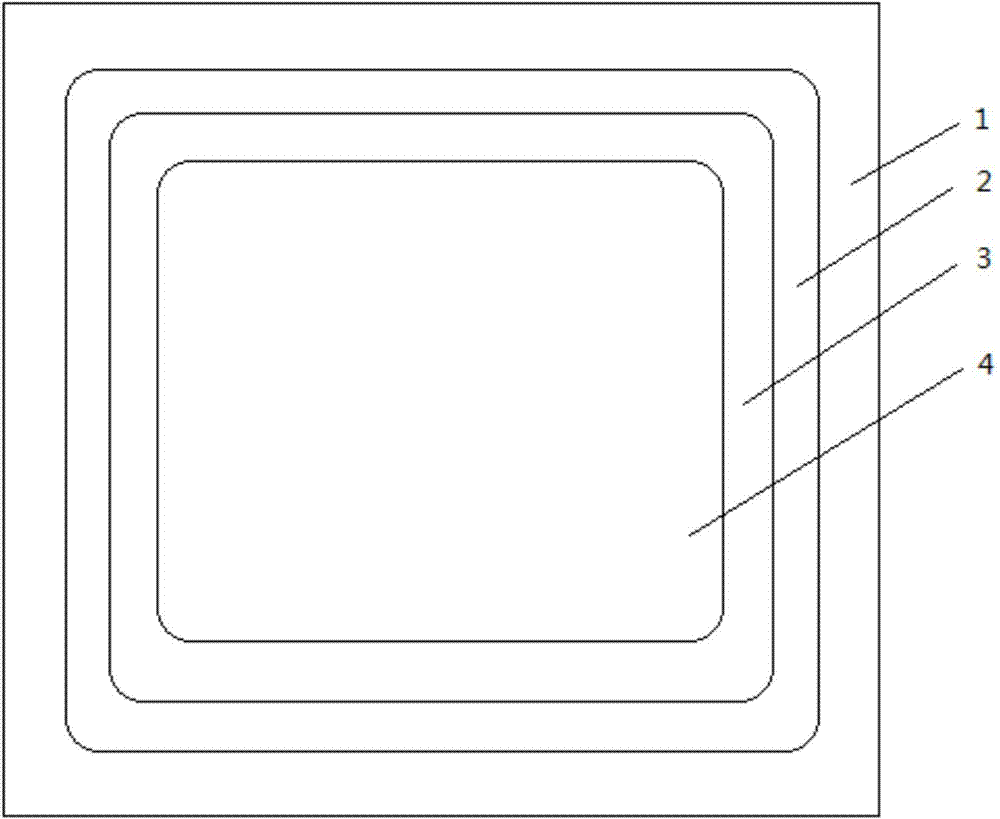
[0066] Such as figure 1 As shown, a Schottky barrier diode chip includes a chip 1, and also includes a terminal groove 2, a protective layer 3 and an electrode 4; the chip 1 is a Schottky barrier diode chip; the electrode 4 is a groove A gate oxide polycrystalline electrode, electrode 4 includes a Schottky region. The Schottky metal in the Schottky area is nickel or chromium, and the electrode 4 of the chip is fused with the Schottky area, so that the chip has a compact structure, better electrical contact performance, and faster chip response during use.

[0067] The protective layer 3 is a PETEOS protective layer 3, which adopts a PETEOS (plasma-enhanced orthoethyl silicate deposition) terminal structure, which reduces the reverse leakage current of the Schottky diode, and the device has better reliability and is suitable for complex environments. The lower diodes are more suitable for use.

[0068] The chip sections are chip 1 , terminal groove 2 , protective layer 3 and ...

Embodiment 2

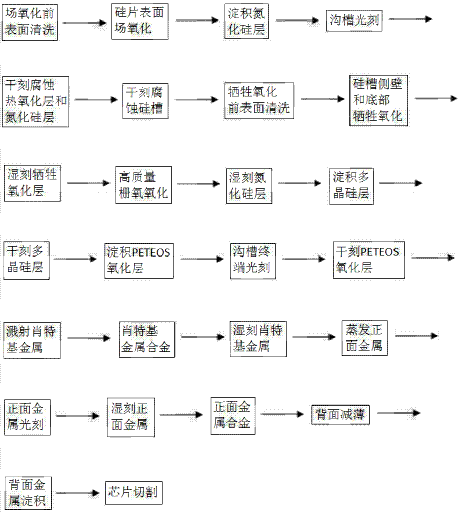
[0112] A production process of a Schottky barrier diode chip, the steps of which are:

[0113] 1) Surface cleaning before field oxidation:

[0114] Configure a hydrofluoric acid solution, which is obtained by mixing a solution with a volume ratio of water:hydrofluoric acid=6:1, and the mass concentration of the hydrofluoric acid solution is 40%;

[0115] Configure No. 1 solution, which is obtained by mixing ammonia water: hydrogen peroxide solution: water = 1:1:5-1:2:7 in volume ratio, and the concentration of ammonia water is 27%;

[0116] Configure No. 2 solution, which is obtained by mixing the volume ratio of hydrogen chloride: hydrogen peroxide solution: water = 1:1:6-1:2:8. The mass concentration of hydrogen chloride is 37%, and the mass concentration of hydrogen peroxide solution is 30%. ;The cleaning sequence is as follows:

[0117] a. Soak the silicon wafer with hydrofluoric acid solution for 30s, and rinse with deionized water;

[0118] b. Soak the silicon wafer w...

Embodiment 3

[0147] Embodiment 3 is basically the same as Embodiment 1, except that the backside thinning method in step 24) is wet etching.


PUM


Abstract

The invention discloses a schottky barrier diode chip and a production technology thereof, and belongs to the field of semiconductor chip production. The schottky barrier diode chip comprises a chip body, a terminal groove, a protecting layer and an electrode. The chip body refers to a schottky barrier diode chip body. The chip section sequentially comprises the chip body, the germinal groove, the protecting layer and the electrode from bottom to top. The electrode refers to a groove gate-oxide polycrystal electrode and comprises a schottky area. The protecting layer refers to a PETEOS (plasma enhanced tetraethoxysilane) protecting layer. Methods such as field surface oxidation, sacrifice oxidation, gate-oxide oxidation, PETEOS oxidation layer deposition, schottky metal sputtering, front metal alloying and back thinning are applied to chip technology improvement. Low switching loss, forward break-over voltage and chip power consumption are achieved, voltage-withstanding stability and reliability of a diode are enhanced, and service life of the diode is prolonged.

Description

technical field [0001] The invention relates to the field of semiconductor chip manufacturing, and more specifically relates to a Schottky barrier diode chip and a production process thereof. Background technique [0002] The development and production of Schottky diodes has a history of more than 20 years. In recent years, with the development of the electronic industry, the unique performance parameters of the first phase of Schottky diodes quickly demonstrated its superiority. In the production of Schottky diodes, there will be many kinds of abnormal breakdowns. When the metal is in contact with the semiconductor, the matching requirements of the Fermi level lead to a potential barrier for charge transfer between the metal and the semiconductor, usually called the Schottky barrier, which is generated due to the different work functions of the metal and the semiconductor. The Schottky diode is made by using the rectification characteristics of the Schottky barrier. It has...

Claims


Application Information

Patent Timeline
Patent Type & Authority Applications(China)
IPC IPC(8): H01L27/095H01L29/40H01L21/28H01L21/82
Inventor 孙澜朱军刘韵吉杨敏红单慧
Owner 桑德斯微电子器件(南京)有限公司
Why Eureka
Try Eureka