
A flexible copper-based chalcogenide semiconductor thin film solar cell window layer structure

A thin-film solar cell and semiconductor technology, applied in the field of solar cells, can solve the problems of reducing the cost of solar cells, poor bending resistance of the film layer, and large physical damage, and achieve the effects of avoiding battery short circuit, small reflection loss, and small physical damage

Active Publication Date: 2017-03-22
CENT SOUTH UNIV
View PDF3 Cites 0 Cited by
  • Summary
  • Abstract
  • Description
  • Claims
  • Application Information

AI Technical Summary

Problems solved by technology

[0005] In view of the defects of poor bending resistance of the film layer, large physical damage during the sputtering process, and high cost in the window layer of the flexible solar cell in the prior art, the purpose of the present invention is to provide a graphene material that replaces components including high-resistance intrinsic ZnO The brittle window layer of thin film and low-resistance transparent conductive oxide is used to obtain a window layer structure of copper-based chalcogenide semiconductor thin film solar cells with good flexibility, and the window layer structure of copper-based chalcogenide semiconductor thin film solar cells avoids the sputtering method. Physical damage to the underlying film when the window layer is used, and greatly reduces the cost of solar cells

Method used


Image

  • A flexible copper-based chalcogenide semiconductor thin film solar cell window layer structure
  • A flexible copper-based chalcogenide semiconductor thin film solar cell window layer structure
  • A flexible copper-based chalcogenide semiconductor thin film solar cell window layer structure

Examples


Embodiment 1

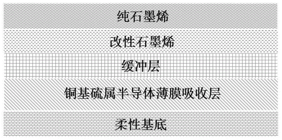
[0024] Design and fabricate the window layer structure of flexible copper-based chalcogenide semiconductor thin film solar cells (as shown in the schematic figure 1shown). The oxidation-reduction method is used to add 4g of flake graphite, 72mL of concentrated sulfuric acid and 36mL of concentrated nitric acid into a beaker in an ice-water bath and stir until it is dispersed. Then slowly add 44g of potassium chlorate. After reacting for 100 hours, add dilute hydrochloric acid solution to dilute and suction filter several times. The filtered product was diluted with deionized water and sonicated for 1 h, then added with sodium hydroxide for flocculation, filtered with suction, washed with absolute ethanol until neutral and then dried to obtain graphene oxide. After the prepared graphene oxide and ammonium chloride are mixed at a mass ratio of 1:2, they are first pyrolyzed at 150-300°C for 1 hour under negative pressure, so that N atoms are doped in the graphene skeleton, and th...

Embodiment 2

[0026] Design and fabricate the window layer structure of flexible copper-based chalcogenide semiconductor thin film solar cells. Using high-purity Cu foil (purity >99%) as the growth substrate, using methane as the carbon source in a tube furnace, and the carrier gas as the reducing gas H 2 , Graphene was prepared by CVD growth at 1000 °C, and polymethyl methacrylate (PMMA) was coated on the copper foil with graphene and then put into FeCl 3 In the solution to remove metal copper foil, obtain graphene (square resistance is 9Ωsq -1 , light transmittance of 97%) PMMA. Then the graphene on PMMA was covered with CdS / Cu(Ga,In)Se 2 / Mo, and remove PMMA with acetone, and then CdS / Cu(Ga,In)Se covered with graphene 2 CdS / Cu(Ga,In)Se covered with modified graphene 2 / Mo (i.e. modified graphene / CdS / Cu(Ga,In)Se 2 / Mo), the square resistance of modified graphene is 1500kΩsq -1 , The light transmittance is 86%. Then vapor-deposit Ni / Al / Ni top electrode on the modified graphene, and ...

Embodiment 3

[0028] Design and fabricate the window layer structure of flexible copper-based chalcogenide semiconductor thin film solar cells. CdS / CuBiSe 2 / Mo / SS (stainless steel) is the growth substrate, acetylene is used as the carbon source in the tube furnace, and the carrier gas is the reducing gas H 2 , Graphene was prepared by CVD growth at 400°C, and then placed in an ammonia atmosphere at 400°C for 4 hours and then hydrogenated in a 300Hz radio frequency plasma apparatus at 1 mbar for 2 hours to obtain a surface covered with modified graphene CdS / CuBiSe 2 / Mo / SS (stainless steel) (i.e. modified graphene / CdS / CuBiSe 2 / Mo / SS (stainless steel)), the square resistance of modified graphene is 1100kΩsq -1 , The light transmittance is 83%. Then prepare the graphene dispersion in the same way as in Example 1 and drop-coat it on the modified graphene, and dry it at 80° C. for 30 min to obtain a flexible graphene window layer copper-bismuth-selenium thin-film solar cell, and obtain a tr...


PUM


Abstract

The invention discloses a flexible copper-based chalcogenide semiconductor thin-film solar cell window layer structure. The structure is formed by arranging a flexible substrate, a copper-based chalcogenide semiconductor thin-film absorption layer, a buffering layer and a window layer sequentially from bottom to top, wherein the window layer is a composite layer composed of a graphene layer and a modified graphene layer which is subjected to doping, hydrogenation and photo-etching or edge modification. According to the flexible copper-based chalcogenide semiconductor thin-film solar cell window layer structure, a brittle window layer comprising a high-resistance intrinsic ZnO thin film and low-resistance transparent conductive oxide is replaced by the graphene composite layer, in this way, the problem that the bending resistance of a flexible solar cell is poor can be effectively solved, and the physical damage to an underling film in the process of manufacturing the window layer based on an existing sputtering method is avoided; meanwhile, the cost of solar cells is greatly reduced, and the industrial mass production requirements are met.

Description

technical field [0001] The invention relates to a flexible copper-based chalcogenide semiconductor thin-film solar cell window layer structure, which belongs to the field of solar cells. Background technique [0002] Flexible solar cells are a type of thin film solar cells. It uses a flexible substrate to replace the traditional glass substrate, which can be bent and folded for easy portability. Its advantages are soft in shape, adjustable in size, light and thin, safe and environmentally friendly. Because of its flexibility, thin-film solar cells can be pasted on objects of any shape, such as the surface of cars, interior walls of homes, and exterior walls of homes. Its applications include building-integrated photovoltaics, solar backpacks, solar convertibles, and solar flashlights. Flexible solar cells can be prepared in a roll-to-roll manner, and have the potential for industrial mass production. [0003] However, at present, the window layer of flexible solar cells i...

Claims


Application Information

Patent Timeline
Patent Type & Authority Patents(China)
IPC IPC(8): H01L31/0216
CPCH01L31/02167Y02E10/50
Inventor 赖延清杨佳蒋妍张坤赵联波蒋良兴李劼刘业翔刘芳洋
Owner CENT SOUTH UNIV
Learn More