High-light-transmittance and low-radiation self-cleaning glass
A technology with high light transmittance and low radiation, which is applied in the field of new building materials and photovoltaic technology, can solve the problems of lower photoelectric conversion efficiency of modules, insufficient energy saving and environmental protection in the construction field, and decreased transparency, so as to improve photoelectric conversion efficiency and reduce Reflectivity, the effect of safety and environmental protection in the production process
- Summary
- Abstract
- Description
- Claims
- Application Information
AI Technical Summary
Problems solved by technology
Method used
Image
Examples
Embodiment 1
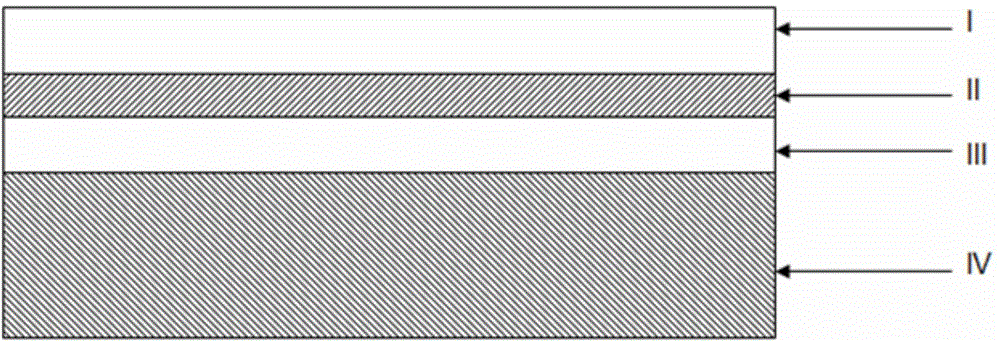
[0013] Implementation example 1 : 5 mm thick float ultra-white glass is used as the base layer, which is cleaned and dried before use; using magnetron sputtering technology, after vacuuming meets the requirements, it passes through magnesium target, titanium-silicon alloy target, titanium-europium in sequence Alloy target, and high-purity argon gas, argon-fluorine mixed gas, argon-oxygen mixed gas are evenly injected at one time, and the structure can be formed as the base layer (5 mm float ultra-clear glass) and the dielectric layer 3 by adjusting the power and gas concentration. (material is magnesium fluoride, thickness 5~350nm), dielectric layer 2 (material is titanium silicon oxide, thickness 10~150nm), dielectric layer 1 (material is silicon europium oxide, thickness 15~200nm) coated glass , this kind of glass has a transmittance of 95% for visible light, a reflectivity of 2%, and a reflectivity of 72% for infrared bands.
Embodiment 2
[0014] Implementation example 2 : 5 mm thick float white glass is used as the base layer, after cleaning and drying, it is ready for use; after the magnetron sputtering process is used, after vacuuming meets the requirements, it goes through vacuum sputtering indium tin coating chamber, vacuum sputtering plasma enhanced deposition Titanium-silicon chamber, vacuum sputtering plasma enhanced deposition titanium-erbium chamber, by adjusting the power and gas concentration, the base layer (5mm float white glass) and the dielectric layer 3 (material is indium tin oxide, thickness 5~350nm) can be formed , Dielectric layer 2 (made of titanium silicon oxide, thickness 10~150nm), dielectric layer 1 (material made of silicon erbium oxide, thickness 15~200nm) of coated glass, the transmittance of this glass to visible light is up to 91 %, the reflectance is 3%, and the reflectance in the infrared band is 73%.
PUM
| Property | Measurement | Unit |
|---|---|---|
| thickness | aaaaa | aaaaa |
| thickness | aaaaa | aaaaa |
| thickness | aaaaa | aaaaa |
Abstract
Description
Claims
Application Information
