

Organic light-emitting device and making method thereof
An electroluminescent device and electroluminescent technology, which are applied in the directions of organic light-emitting devices, organic light-emitting device structures, organic semiconductor devices, etc., can solve the problems of organic layer damage, low luminous efficiency, easy quenching, etc.
- Summary
- Abstract
- Description
- Claims
- Application Information
AI Technical Summary
Problems solved by technology
Method used
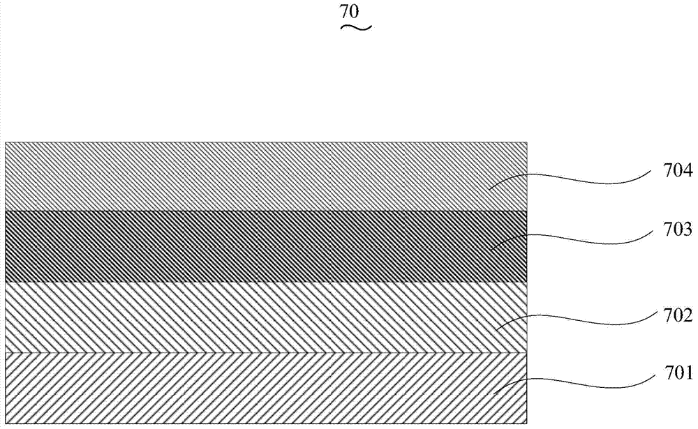
Image

Examples
preparation example Construction
[0033] The preparation method of the organic electroluminescence device 100 of an embodiment, it comprises the following steps:
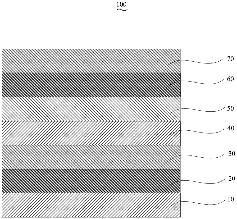
[0034] Step S110 , sequentially forming a hole injection layer 20 , a hole transport layer 30 , a light emitting layer 40 , an electron transport layer 50 and an electron injection layer 60 on the surface of the anode 10 .
[0035] The anode 10 is indium tin oxide glass (ITO), fluorine-doped tin oxide glass (FTO), aluminum-doped zinc oxide glass (AZO) or indium-doped zinc oxide glass (IZO), preferably ITO.
[0036] In this embodiment, before the hole injection layer 20 is formed on the surface of the anode 10, the anode 10 is pretreated. The pretreatment includes: performing photolithography on the anode 10, cutting it into the required size, using detergent, deionized Water, acetone, ethanol, and isopropanone were each ultrasonically cleaned for 15 minutes to remove organic pollutants on the surface of the anode 10 .
[0037] The hole injection la...
Embodiment 1
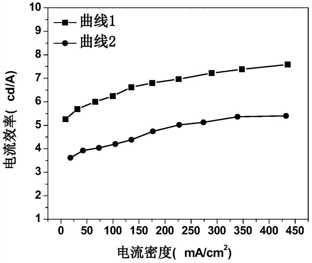
[0051] The structure prepared in this example is ITO / WO 3 / NPB / Alq 3 / Bphen / LiF / TAZ:MoO 3 / Ta 2 o 5 The organic electroluminescent device of / Ag / ZnS / , in this embodiment and the following embodiments, " / " indicates a layer, and ":" indicates doping.
[0052] First, carry out photolithography treatment on ITO, cut it into the required size, and then use detergent, deionized water, acetone, ethanol, and isopropanol to sonicate for 15 minutes each to remove organic pollutants on the glass surface; clean the conductive substrate Carry out suitable treatment: oxygen plasma treatment, treatment time is 5min, power is 30W; evaporation hole injection layer, material is WO 3 , with a thickness of 35nm; the vapor-deposited hole transport layer, the material is NPB, and the thickness is 40nm; the vapor-deposited light-emitting layer, the material is Alq 3 , thickness is 15nm; Evaporation electron transport layer, material is Bphen, thickness is 250nm; Evaporation electron injection ...
Embodiment 2
[0059] The structure prepared in this example is AZO / MoO 3 / NPB / ADN / TAZ / CsF / OXD-7:WO 3 / Nb 2 o 5 / Al / CdS organic electroluminescent devices.
[0060] First, use detergent, deionized water, and ultrasonication on the AZO glass substrate for 15 minutes to remove organic pollutants on the glass surface; evaporate the hole injection layer: the material is MoO 3 , the thickness is 80nm; evaporation hole transport layer: the material is NPB, the thickness is 60nm; evaporation light-emitting layer: the selected material is ADN, the thickness is 5nm; evaporation electron transport layer, the material is TAZ, the thickness is 75nm; The electron injection layer is plated, the material is CsF, and the thickness is 10nm; the evaporation cathode is evaporated on the surface of the electron injection layer by thermal resistance evaporation to prepare an organic electron transport doped layer, and the material is OXD-7:WO 3 , OXD-7 and WO 3 The mass ratio is 2:1, the thickness is 50nm, ...
PUM
 Abstract
Description
Claims
Application Information