Surface grid-type static induction transistor

An electrostatic induction and transistor technology, applied in the direction of transistors, circuits, electrical components, etc., can solve the problems of large gate cut-off current and drain cut-off current, weakened gate control sensitivity, low gate-source breakdown voltage, etc., to reduce gate-source parasitic capacitance , increasing gate control sensitivity and reducing gate-source area

Inactive Publication Date: 2015-07-29
LANZHOU UNIVERSITY
View PDF5 Cites 4 Cited by
  • Summary
  • Abstract
  • Description
  • Claims
  • Application Information

AI Technical Summary

Problems solved by technology

However, the impurity concentration formed by diffusion high-temperature annealing in this invention is a Gaussian distribution, and the design of the long channel in the active region makes the concentration of the gate body vary greatly, and the gate body itself will form a potential drop to weaken the regulation of the external gate voltage, and at the same time The large concentration drop makes the effective channel length much smaller than the actual channel length, and the long-term high-temperature advancement reduces the gate body concentration, which will greatly weaken the gate control sensitivity
In addition, the advance speed of thermal diffusion in silicon is very slow, and the diffusion speed in each direction is different. It is easy to form a spherical or elliptical diffusion junction with curved edges. Concentrated or divergent, which reduces the breakdown voltage
Moreover, the advance of thermal annealing leads to severe lateral diffusion in the active region. To prevent gate-source short circuit, the device gate spacing must be increased, thereby increasing the device size, reducing wafer utilization, and increasing manufacturing costs.
[0005] At present, there are several long-channel SITs that have been commercialized in foreign countries, such as the 2SK79 V FET produced by Japan's SONY company, but their prices are high and it is difficult to obtain them in the domestic market. to buy
In addition, its performance also has some shortcomings: low gate-source breakdown voltage (BVgso=10V), large gate cut-off current and drain cut-off current (Igso=200nA, Idgo=200nA), low voltage amplification factor (μ=30), crossover Low conduction (gm=30mS), large package area (8.7mm×6.0mm), etc.

Method used


Image

  • Surface grid-type static induction transistor
  • Surface grid-type static induction transistor
  • Surface grid-type static induction transistor

Examples


Embodiment Construction

[0044] The present invention is explained in detail below.

[0045] The process of the present invention is compatible with the traditional planar CMOS process, and the entire manufacturing process is as follows:

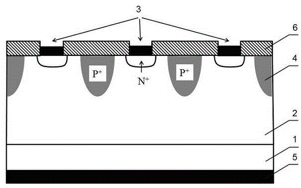
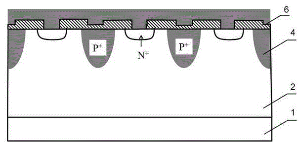
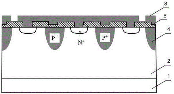
[0046] Silicon wafer cleaning - thermal oxidation - one photolithography (gate area, source area, gate wall window) - second photolithography (gate area, gate wall) - boron injection - one annealing - three photolithography - —Arsenic injection—second annealing (RTP)—LPCVD oxidation—densification annealing—four photolithography (ohmic contact window)—metallization—anti-etch gold—deposition of composite dielectric—five times Photolithography (lead hole) - triple annealing - backside thinning - backside metallization - dicing - packaging.

[0047] The invention can be formed by connecting 1500 to 2000 SIT units in parallel, and the current density of the device is greatly improved.

[0048] The following is an embodiment of the present invention, which will be descr...


PUM


Abstract

The invention relates to a normally closed surface grid-type static induction transistor (SIT) of low power and a manufacturing method. The transistor is formed by parallelly connecting a drain electrode, a substrate of N+ low resistance monocrystal located on the drain electrode, an N- high resistance epitaxial layer located on the substrate of N+ low resistance monocrystal and multiple mutually parallelly-connected SIT units located in the N- high resistance epitaxial layer, wherein the active region uses the short channel design. The transistor is capable of enabling the impurity concentration of the device grid body to be high and enabling the impurity distribution to be more uniform under the corresponding technology support, reducing the own voltage drop of the grid body, increasing the sensitivity of the grid control, improving the device transconductance, reducing the grid source area, reducing the stray capacitance of the grid source, and increasing the SIT working frequency. Compared with the prior art, the short channel design is completely improved revolutionarily.

Description

technical field [0001] The invention relates to a low-power normally-off electrostatic induction transistor, in particular to a surface gate electrostatic induction transistor. Background technique [0002] In the patent U.S. Patent No.4326209, Nishizawa et al proposed that a static induction transistor (SIT) is a field effect semiconductor device capable of operating under relatively high frequency and high power conditions. In the channel, carriers are injected from the source across a potential barrier induced by channel electrostatics to the drain, and the barrier height can vary with changes in the gate bias applied to the gate and the drain bias applied to the drain . The key to the performance of SIT lies in the channel formed by the high-resistance epitaxial layer that can control the depletion of carriers. It has the advantage that the current-voltage characteristic curve is close to linear in a very wide range of leakage current, including the region of low leaka...

Claims


Application Information

Patent Timeline
Patent Type & Authority Applications(China)
IPC IPC(8): H01L29/772H01L29/08H01L21/335
CPCH01L29/7722H01L29/1029H01L29/66416
Inventor 杨建红王娇乔坚栗闫兆文谌文杰杨盼
Owner LANZHOU UNIVERSITY
Why Eureka
Try Eureka