Novel mold core for optical lens processing and preparation method therefor
A technology of optical lens and mold core, which is applied in the direction of glass pressing, glass manufacturing equipment, manufacturing tools, etc. It can solve the requirements that do not meet the surface quality requirements of high-precision micro-lenses. The light transmittance and performance of plastics are not as good as optical glass, which cannot be realized Extensive processing of optical materials and other issues to achieve the effects of high hardness, good consistency, good compatibility and integration
- Summary
- Abstract
- Description
- Claims
- Application Information
AI Technical Summary
Problems solved by technology
Method used
Image
Examples
Embodiment 1
[0035] Example 1: Ordinary photolithography plus variable speed etching of wafer-level tungsten core array
[0036] 1) Use 4-inch, 6-inch, 8-inch or 12-inch metal tungsten polished discs, and clean the surface;
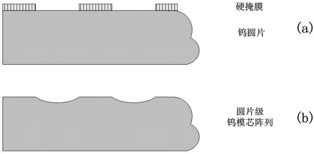
[0037] 2) Photolithography forms a mask for defining the shape of the tungsten core, such as figure 1 As shown in figure (a), the mask can be a photoresist mask or other organic material mask, or a hard mask;
[0038] 3) Under the cover of the above mask, an etching gas (SF 6 and other fluorine-based gases) or a variety of mixed etching gases (SF 6 Fluorine-based gases such as O 2 , N 2 etc.), for variable speed etching of metal tungsten wafers, by controlling the etching type (isotropic, anisotropic), etching rate, etching selection ratio, etc., the wafer-level tungsten mold with the required curvature radius can be designed Core arrays, such as figure 1 As shown in (b) figure:
[0039] The mask is formed by a common photolithography process, and the etching g...
Embodiment 2
[0042] Example 2: The photoresist of the wafer-level tungsten mold core is melted and reflowed, photolithography is added and etched at a constant speed, and a spherical wafer-level tungsten mold core array is processed and prepared;
[0043] 1) Use 4-inch, 6-inch, 8-inch or 12-inch metal tungsten polished discs, and clean the surface;
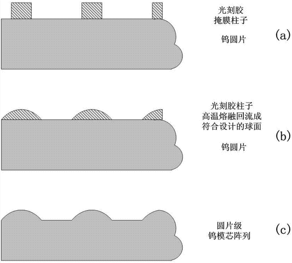
[0044] 2) Photolithography forms a photoresist cylinder used to define the shape of the tungsten core, such as figure 2 As shown in (a) in the figure, by means of high-temperature melting reflow process, by controlling temperature and time, a spherical photoresist mask with a radius of curvature that meets the design requirements is formed, such as figure 2 As shown in (b) figure;
[0045] 3) Under the cover of the above photoresist mask, a single component (SF 6 Fluorine-based gases) or multi-component etching gases (SF 6 Fluorine-based gases such as O 2 , N 2 etc.), adjust the appropriate gas ratio and etching parameters (gas flow, po...
Embodiment 3
[0047] Embodiment 3: Special photolithography plus uniform-speed etching of wafer-level tungsten mold cores to process and prepare spherical wafer-level tungsten mold core arrays;
[0048] 1) Use 4-inch, 6-inch, 8-inch or 12-inch metal tungsten polished discs, and clean the surface;
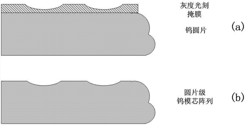
[0049] 2) The etching mask is formed by special lithography process, including: gray scale lithography, electron beam lithography, laser lithography, mask moving lithography, moving mask filtering technology, etc., forming a mask with specific optical information film, such as image 3 As shown in (a) figure (this figure represents the mask formed by grayscale lithography);
[0050] 3) Under the cover of the above photoresist mask, a single component (SF 6 Fluorine-based gases) or multi-component etching gases (SF 6 Fluorine-based gases such as O 2 , N 2 etc.), adjust the appropriate gas ratio and etching parameters (gas flow, power, etc.) to achieve an appropriate etching rate, etch the waf...
PUM
 Abstract
Description
Claims
Application Information


