Middle-high temperature thermoelectric module
A technology of thermoelectric modules and electric modules, which is applied in the directions of thermoelectric device parts, thermoelectric device manufacturing/processing, thermoelectric devices using only Peltier or Seebeck effect, etc. Diffusion and other problems, to achieve the effect of good continuity, good use effect and economic value, environmental protection benefit and excellent insulation performance
- Summary
- Abstract
- Description
- Claims
- Application Information
AI Technical Summary
Problems solved by technology
Method used
Image
Examples
preparation example Construction
[0054] The invention provides a method for preparing a thermoelectric device. In order to further improve the conversion efficiency of the thermoelectric device, an anti-oxidation layer with strong adhesion, high density and good continuity is formed on the outer layer or outer layers by physical or chemical methods. Sublimation diffusion barrier protective layer, and this layer has the excellent performance of long service life and strong heat aging resistance.
[0055] The outside of the diffusion barrier protection layer is a thermal insulation layer composed of aerogel or aerogel composite material, while the inner layer and / or outer layer is one or more layers of metal layer, the metal transition layer can prevent The high-temperature volatilization of the Sb element can also increase the bonding strength between the oxide layer and the skutterudite material.
[0056] The heat insulation layer adopts airgel or fiber composite airgel or ceramic powder composite airgel. Th...
Embodiment 1
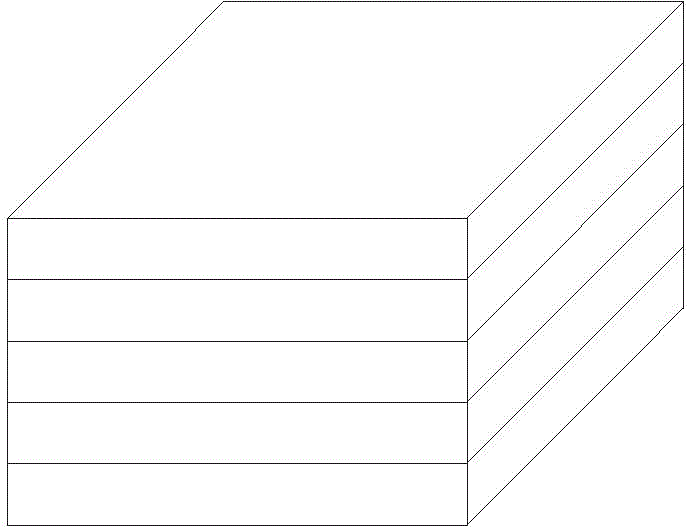
[0085] Sintered dense thermoelectric materials such as n-type Yb 0.3 co 4 Sb 12 , p-type CeFe 3 CoSb 12 And cut into thin slices of equal thickness, the relative density is greater than 96% (see figure 1 );
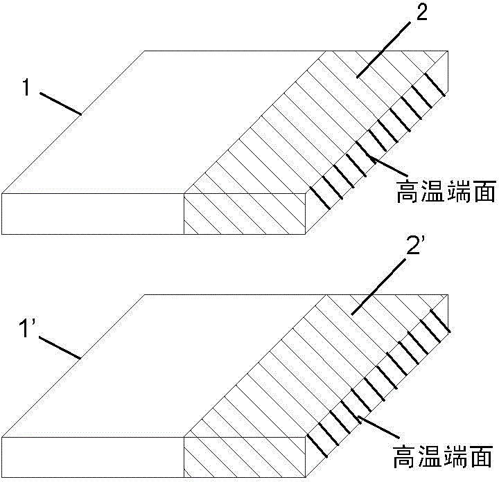
[0086] Cover the low-temperature end with a mask, and only sputter Mo, Cr, etc. on the high-temperature end to prevent the diffusion barrier protective layer from Sb diffusion (see figure 2 );
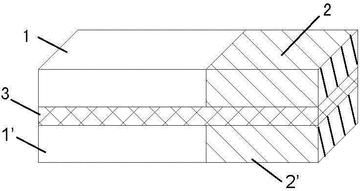
[0087] Connect the p-type and n-type materials sputtered with a diffusion barrier protection layer with an insulating high-temperature-resistant adhesive, such as nano-SiO modified by methyl silicone resin 2 adhesive (see image 3 );
[0088] Polymer-assisted deposition to prepare diffusion barrier protective layers, such as Ti film, W film, etc.;
[0089] Put the n-p material into the mold, magnetron sputtering diffusion barrier buffer layer Ti, Mo, etc., and then add a small amount of Ti powder on the diffusion barrier buffer layer, and sinter the high-temperature end ...
Embodiment 2
[0093] Sintered dense p- or n-type thermoelectric blocks with a relative density of >96% and a size of 13×13×4mm;
[0094] Wire cutting into three thermoelectric pins with a size of 4×4×13mm, after surface polishing, sequentially sputter Mo, Si and other diffusion barrier protective layers. The sputtering process of the Mo layer is as follows: Ar flow rate 80sccm, DC power 200W, substrate temperature 673K, sputtering time 30min, ignition pressure 5Pa, background vacuum better than 5.0×10 -4 The thickness of the Pa and Mo layers is about 1 μm. The sputtering process of the Si layer is as follows: Ar flow rate 80sccm, DC power 200W, substrate temperature 673K, sputtering time 80min, ignition pressure 7Pa, background vacuum better than 5.0×10 -4 Pa, Si layer thickness is about 500nm;
[0095] Silica sol nanophase binder modified with siloxane via SiO 2 , ZrO 2 After airgel recombination, thermoelectric bulk materials sputtered with protective films of Mo and Si were connected...
PUM
| Property | Measurement | Unit |
|---|---|---|
| thickness | aaaaa | aaaaa |
| thickness | aaaaa | aaaaa |
| thickness | aaaaa | aaaaa |
Abstract
Description
Claims
Application Information


