Preparation method of Si-ITO composite nanowire ordered array

A nanowire array and ordered array technology is applied in the field of preparation of Si-ITO composite nanowire ordered arrays, and achieves the effects of stable performance, uniform diameter and good repeatability

Inactive Publication Date: 2015-09-30
XI AN JIAOTONG UNIV
View PDF3 Cites 5 Cited by
  • Summary
  • Abstract
  • Description
  • Claims
  • Application Information

AI Technical Summary

Problems solved by technology

In the prior art, most of the growths on Si nanowires are ZnO (zinc oxide) nanostructures, while the grown ITO materials are all thin film structures. There is no report on the synthesis of ordered arrays of Si-ITO composite nanowires.

Method used


Image

  • Preparation method of Si-ITO composite nanowire ordered array
  • Preparation method of Si-ITO composite nanowire ordered array
  • Preparation method of Si-ITO composite nanowire ordered array

Examples


preparation example Construction

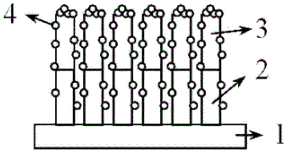
[0032] A preparation method of a Si-ITO composite nanowire ordered array of the present invention comprises the following steps:

[0033] The first step: the cleaning process of the nanowire substrate.

[0034] 1.1), put the nanowire substrate 1 (single crystal silicon wafer) into chloroform for ultrasonic cleaning for 10 minutes to remove the organic residue on the silicon surface;

[0035] 1.2), put the nanowire substrate 1 into deionized water and ultrasonicate for about 5 minutes, remove the residual chloroform, and then dry it with nitrogen;

[0036] 1.3), put the nanowire substrate 1 into the hydrofluoric acid (HF) with a concentration of 10% for 30s, and remove the oxidized silicon dioxide on the surface of the nanowire substrate 1;

[0037] 1.4) Put the nanowire substrate 1 into deionized water for ultrasonic cleaning for 5 minutes to remove residual HF, and then dry it with nitrogen.

[0038] The second step: the preparation of Si nanowires.

[0039] The Si nanowir...

Embodiment 1

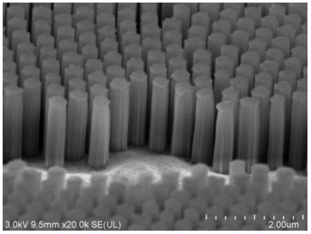
[0050] On the surface of the cleaned single crystal p-type (100) Si wafer, a single layer of PS spheres with a diameter of 670 nm was self-assembled, and the PS spheres were etched with oxygen by an inductively coupled plasma (ICP) etching machine for 200 s. The diameter of the PS pellets became -500 nm, followed by vapor deposition of metallic silver. Set the evaporation current to 115A and the evaporation rate to be The evaporation chamber pressure is 7×10 -4 Pa, the thickness of the vapor-deposited silver film is 40nm, then the silicon wafer is placed in chloroform solution, soaked for 15 minutes under ultrasonic conditions to remove PS pellets, and then the sample silicon wafer is placed in deionized water for ultrasonic cleaning for 5 minutes , to remove the residual chloroform solution, and dry naturally under nitrogen atmosphere. At this time, a silver mesh film has been formed on the surface of the sample silicon wafer.

[0051] Configure an etching solution of hyd...

Embodiment 2

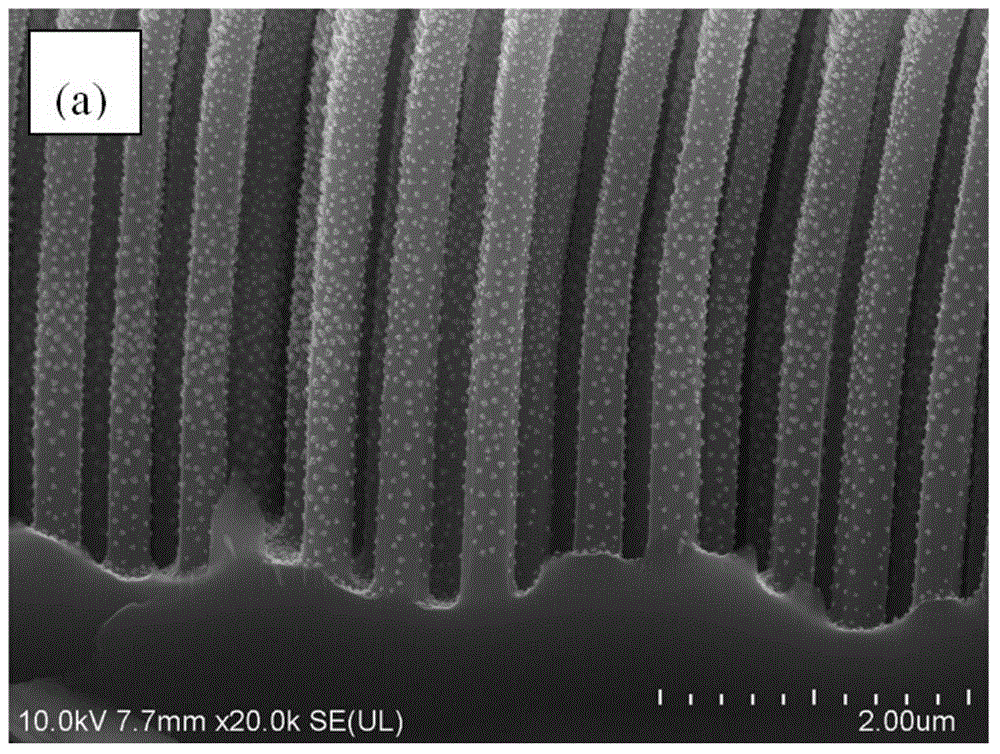
[0054] After self-assembly of PS beads with a monolayer diameter of 500 nm on the surface of the cleaned Si wafer, the PS beads were etched with oxygen for 150 s using an inductively coupled plasma (ICP) etcher, and the diameter of the PS beads became ~ 350 nm, followed by vapor deposition of metallic silver. Set the evaporation current to 115A and the evaporation rate to be The evaporation chamber pressure is 7×10 -4 Pa, the thickness of the vapor-deposited silver film is 35nm, then the silicon wafer is placed in chloroform solution, soaked for 15 minutes under ultrasonic conditions to remove PS pellets, and then the sample silicon wafer is placed in deionized water for ultrasonic cleaning for 5 minutes , to remove the residual chloroform solution, and dry naturally under nitrogen atmosphere. At this time, a silver mesh film has been formed on the surface of the sample silicon wafer.

[0055] Configure an etching solution of hydrofluoric acid (HF): hydrogen peroxide (H2O2...


PUM

PropertyMeasurementUnit
diameteraaaaaaaaaa
diameteraaaaaaaaaa
lengthaaaaaaaaaa

Abstract

The invention discloses a preparation method of a Si-ITO composite nanowire ordered array. The method comprises the following steps: etching a structured and ordered Si nanowire array on a clean monocrystalline silicon chip by using a dry-wet etching combination process, and growing ITO nanowires in an ITO electron beam vapor plating mode according to an autocatalysis principle to realize seamless combination of Si nanowires and the ITO nanowires in order to obtain the Si-ITO composite nanowire ordered array. The obtained Si-ITO nanowires have the advantages of uniform diameter, adjustable proportion, and coverage of the surface and the front of the Si-ITO nanowires by ITO grains. The method has the characteristics of simple operation, concise preparation process, good repeatability, stable performance and strong compounding property. The composite nanowires have good application prospects in the fields of nanocrystalline solar batteries, nanometer sensors and field emission display.

Description

【Technical field】 [0001] The invention belongs to the technical field of semiconductor materials, and in particular relates to a preparation method of an ordered array of Si-ITO (silicon-indium tin oxide) composite nanowires. 【Background technique】 [0002] One-dimensional nanowires have the characteristics of large specific surface area, good assembly performance and microscopic one-dimensional structure. Composite nanowires are widely used in optics, catalysis, adsorption, detection and other fields because they have the physical and chemical properties of two or more one-dimensional nanomaterials, and have tunable one-dimensional properties. A research hotspot in the field of materials. [0003] Si nanowire materials with one-dimensional structures have important practical applications in optoelectronic devices such as field emission devices, single-electron memory devices, high-efficiency lasers, nanosensors, and solar cells. ITO material is a wide-bandgap semiconducto...

Claims


Application Information

Patent Timeline
Patent Type & Authority Applications(China)
IPC IPC(8): C23C14/30C23C14/08C30B33/08B82Y40/00
Inventor 李强弓志娜云峰
Owner XI AN JIAOTONG UNIV
Why Eureka
Try Eureka