Production method of GaN-based white LED epitaxial structure

An epitaxial structure, white light technology, applied in the direction of chemical instruments and methods, crystal growth, electrical components, etc., can solve the problems of uneven phosphor material, device color shift, thermal degradation, etc., to achieve simplified manufacturing process and good color temperature control , the effect of improving stability

Active Publication Date: 2015-09-30
XI AN JIAOTONG UNIV
View PDF4 Cites 7 Cited by
  • Summary
  • Abstract
  • Description
  • Claims
  • Application Information

AI Technical Summary

Problems solved by technology

Since the gap between the phosphor powder and the LED chip is filled with a gas or colloid with low thermal conductivity, the heat in the phosphor material cannot be effectively dissipated through the heat sink of the LED package, which will also cause color shift of the device, decrease in luminous efficiency, and shorten the life of the device.
[0006] Therefore, there is an urgent need for a new white LED manufacturing process to solve the phenomenon of uneven phosphor material and thermal degradation, while simplifying the packaging process, improving yield, and reducing production costs.

Method used


Image

  • Production method of GaN-based white LED epitaxial structure

Examples


Embodiment 1

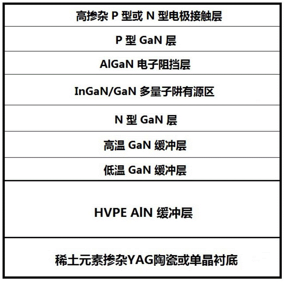
[0032] Take a Ce:YAG single crystal substrate with a doping concentration of 0.3 at%, a thickness of 500 μm, and a surface roughness of less than 0.5 nm, and put it into the reaction chamber of a hydride vapor phase epitaxy (HVPE) equipment after cleaning. Introduce hydrogen (H 2 ) high temperature baking for 10 minutes, the baking temperature is 1200 ℃, and then ammonia gas (NH 3 ) Nitriding the substrate surface at 1300° C. for 20 minutes.

[0033] Ammonia gas (NH 3 ) and carrier gas nitrogen, the hydrogen chloride (HCl) with a flow rate of 100 sccm is passed into the aluminum source area, the reaction generates a hydride source and is passed into the reaction chamber, the temperature of the aluminum source area is 550 ° C, and the carrier gas of hydrogen chloride (HCl) is Nitrogen, flow 2000sccm. In the reaction chamber, the hydride source and ammonia gas (NH 3 ) and grow a 100nm height (002) oriented polycrystalline AlN buffer layer on the substrate. Wherein, the temp...

Embodiment 2

[0036] Take a piece of Eu:YAG ceramic substrate with a doping concentration of 0.5 at%, a thickness of 100 μm, and a surface roughness of less than 0.5 nm, and put it into the reaction chamber of a hydride vapor phase epitaxy (HVPE) equipment after cleaning. Introduce hydrogen (H 2 ), baked at 800°C for 20 minutes, and then passed ammonia gas (NH 3) for 60 minutes of substrate surface nitriding treatment, and the nitriding temperature is 1300°C. Ammonia gas (NH 3 ) and carrier gas nitrogen, the hydrogen chloride (HCl) with a flow rate of 50 sccm is passed into the aluminum source area, the reaction generates a hydride source and is passed into the reaction chamber, the temperature of the aluminum source area is 450 ° C, and the carrier gas of hydrogen chloride (HCl) is Nitrogen, flow rate 1000sccm. In the reaction chamber, the hydride source and ammonia gas (NH 3 ) and grow a 5nm (002) single crystal AlN buffer layer on the substrate. Wherein, the temperature of the react...

Embodiment 3

[0038] Take a Nd:YAG ceramic substrate with a doping concentration of 0.05at%, a thickness of 1000 μm, and a surface roughness of less than 0.5 nm, and put it into a reaction chamber of a hydride vapor phase epitaxy (HVPE) equipment after cleaning. Introduce hydrogen (H 2 ), baked at 1400°C for 5 minutes, and then passed ammonia gas (NH 3 ) for 3 minutes of substrate surface nitriding treatment, and the nitriding temperature is 1500°C. Ammonia gas (NH 3 ) and carrier gas hydrogen, the hydrogen chloride (HCl) with a flow rate of 300 sccm is passed into the aluminum source area, the reaction generates a hydride source and is passed into the reaction chamber, the temperature of the aluminum source area is 600 ° C, and the carrier gas of hydrogen chloride (HCl) is Hydrogen, flow 2000sccm. In the reaction chamber, the hydride source and ammonia gas (NH 3 ) and grow a 20nm (002) oriented polycrystalline AlN buffer layer on the substrate. Wherein, the temperature of the reaction...


PUM

PropertyMeasurementUnit
thicknessaaaaaaaaaa
surface roughnessaaaaaaaaaa
thicknessaaaaaaaaaa

Abstract

A production method of a GaN-based white LED epitaxial structure includes the steps of preparing a monocrystalline or polycrystalline aluminum nitride buffer layer on a rare earth element doped YAG (yttrium aluminum garnet) ceramic or monocrystalline substrate by means of hydride vapor phase epitaxy; growing a GaN-based LED epitaxial structure on the monocrystalline or polycrystalline aluminum nitride buffer layer by means of metal-organic chemical vapor deposition. The GaN-based LED epitaxial structure comprises a low-temperature GaN buffer layer, a high-temperature GaN layer, an N-type GaN layer, an InGaN / GaN multiple quantum well active area, an AlGaN electronic barrier layer, a P-type GaN layer and a high-doped P-type or N-type electrode contact layer sequentially from bottom to top. The GaN-based LED epitaxial structure has the advantages that optical and physical features of fluorescent material, such as doping, thickness and quality, can be accurately controlled, integration of the fluorescent material high in repeatability and uniformity is achieved, and the problem that in traditional phosphor coating, unavailable non-uniform phosphor content occurs to the different parts of a same wafer and the different wafers due to the production process is solved.

Description

Technical field: [0001] The invention relates to the field of optoelectronic technology, in particular to a method for preparing a GaN-based white light LED epitaxial structure. Background technique: [0002] Since Nakamura and others successfully developed GaN blue LEDs in 1991, GaN-based LEDs with excellent characteristics such as high efficiency, small size, long life, and environmental protection have achieved unprecedented development and have extremely broad application prospects. Currently, white LEDs usually use blue LEDs to excite yellow phosphors to generate white light. Phosphor powder coating process can be mainly divided into three types: spraying (dispensing) process on a single packaged blue LED chip, spin coating process on the entire wafer before chip cutting, and adding remote phosphor small plate in the packaging structure technology. [0003] In the traditional spraying (dispensing) process, phosphor powder is mixed with colloid and then coated directly...

Claims


Application Information

Patent Timeline
Patent Type & Authority Applications(China)
IPC IPC(8): H01L33/00C30B25/18
CPCC30B25/18H01L33/007
Inventor 云峰李虞锋张维涵
Owner XI AN JIAOTONG UNIV
Why Eureka
Try Eureka