Amorphous vanadium oxide film material containing V6O13 crystals and preparing method thereof

A technology of V6O13 and vanadium oxide film, which is applied in the field of materials, can solve the problems of impure composition, poor film uniformity, and incompatibility, and achieve the effect of simple preparation process, stable resistance change, and smooth and dense surface

Active Publication Date: 2015-11-04
BEIJING INSTITUTE OF TECHNOLOGYGY
View PDF2 Cites 10 Cited by
  • Summary
  • Abstract
  • Description
  • Claims
  • Application Information

AI Technical Summary

Problems solved by technology

Among them, the uniformity of the film produced by the pulsed laser deposition process is poor, and it can only be produced on a small-area substrate.
It is easy to target poisoning by ion beam deposition and can only be prepared in a small area
Films prepared by the evaporation method have poor adhesion to the substrate and are impure and easily mixed with impurities; films prepared b

Method used


Image

  • Amorphous vanadium oxide film material containing V6O13 crystals and preparing method thereof
  • Amorphous vanadium oxide film material containing V6O13 crystals and preparing method thereof
  • Amorphous vanadium oxide film material containing V6O13 crystals and preparing method thereof

Examples


preparation example Construction

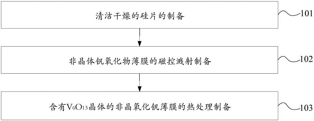
[0034] The present invention provides a kind of containing V 6 o 13 A method for preparing a crystalline amorphous vanadium oxide thin film material. refer to figure 1 , which shows that the preparation of the examples of the present invention contains V 6 o 13 A flowchart of a method for crystalline amorphous vanadium oxide thin films, the method comprising the following steps:

[0035] Step 101, preparation of the clean and dry silicon wafer.

[0036] Preparation of clean and dry silicon wafers: the silicon wafers were sequentially ultrasonically cleaned in concentrated hydrochloric acid with a purity of 99.99%, acetone, absolute ethanol, and deionized water for 20 to 30 minutes to remove impurities on the surface of the silicon substrate, and then cleaned The final silicon substrate is dried for future use.

[0037] The impurities on the surface of the silicon wafer are removed through the above treatment process, which prevents the impurities on the surface of the si...

Embodiment 1

[0054] The following examples all adopt MSP-620 automatic magnetron sputtering apparatus, the target material is a metal vanadium target with a purity of 99.999%, the substrate is a 2-4 inch silicon chip, and the silicon chip is directly sputtered by the metal vanadium target , The purity of oxygen and argon in the sputtering gas is 99.999%.

[0055] The silicon wafer was ultrasonically cleaned for 30 minutes in concentrated hydrochloric acid with a purity of 99.99%, acetone, absolute ethanol and deionized water in sequence, and then dried to obtain a clean and dry silicon wafer.

[0056] Put the clean and dry silicon wafer in the magnetron sputtering vacuum chamber, and evacuate the magnetron sputtering vacuum chamber to 9×10 -4 Pa; argon is the sputtering gas, and oxygen is the reaction gas, which are jointly fed into the chamber. The gas flow of argon is 40 sccm, and the gas flow of oxygen is 0.8 sccm; after feeding argon and oxygen, adjust the magnetron sputtering The vac...

Embodiment 2

[0059] The following examples all adopt MSP-620 automatic magnetron sputtering apparatus, the target material is a metal vanadium target with a purity of 99.999%, the substrate is a 2-4 inch silicon chip, and the silicon chip is directly sputtered by the metal vanadium target , The purity of oxygen and argon in the sputtering gas is 99.999%.

[0060] The silicon wafer was ultrasonically cleaned for 30 minutes in concentrated hydrochloric acid with a purity of 99.99%, acetone, absolute ethanol and deionized water in sequence, and then dried to obtain a clean and dry silicon wafer.

[0061] Put the clean and dry silicon wafer in the magnetron sputtering vacuum chamber, and evacuate the magnetron sputtering vacuum chamber to 0.5×10 -5Pa; the sputtering gas is argon, and oxygen is a reaction gas, which are jointly fed into the chamber, and the gas flow of argon is 55 sccm, and the gas flow of oxygen is 1.4 sccm; The vacuum degree in the vacuum chamber is 2Pa, the sputtering power...


PUM

PropertyMeasurementUnit
Room temperature resistanceaaaaaaaaaa
Temperature coefficient of resistanceaaaaaaaaaa

Abstract

The invention provides an amorphous vanadium oxide film material containing V6O13 crystals and a preparing method thereof. The method comprises the following steps: preparing a clean and dry silicon wafer; in a sputtering process, simultaneously introducing a metallic vanadium target used as a target material, the clean and dry silicon wafer used as a substrate, argon used as sputtering gas and oxygen used as reaction gas into a magnetically-controlled sputtering chamber, and depositing an amorphous vanadium oxide film on the silicon substrate; and placing the prepared amorphous vanadium oxide film into a vacuum annealing furnace so as to carry out thermal treatment, and after thermal treatment, obtaining the amorphous vanadium oxide film material containing the V6O13 crystals. According to the preparing method provided by the invention, the prepared film material has neat and compact surfaces and relatively uniform material particles. Meanwhile, the resistance of the produced film material is moderate and sensitive with temperature variation, the temperature coefficient of the resistance is larger than 2%/K, and the variation of the resistance is stable in heating and cooling processes. The amorphous vanadium oxide film material can be used for manufacturing a micro-bolometer.

Description

technical field [0001] The present invention relates to the technical field of materials, in particular to a 6 o 13 Crystalline amorphous vanadium oxide film material, and a V 6 o 13 A method for preparing a crystalline amorphous vanadium oxide thin film material. Background technique [0002] Vanadium oxide film VO x As a heat-sensitive material, due to its low room temperature resistance, high temperature coefficient of resistance (TCR) value (about 2.0% / K, 5-10 times higher than most metals), preparation process compatible with silicon process and its The manufactured device has the characteristics of low 1 / f noise and high frame number (60HZ), and has been widely concerned and researched in recent years. . [0003] But generally speaking, there is a mutual restrictive relationship between the resistance value of the film and the temperature coefficient of resistance (TCR). A film with a large TCR value also has a large resistance value, and the TCR will also decrea...

Claims


Application Information

Patent Timeline
IPC IPC(8): C23C14/08C23C14/35C23C14/58
Inventor 李静波苏玉玉金海波豆艳坤
Owner BEIJING INSTITUTE OF TECHNOLOGYGY
Why Eureka
Try Eureka