Cr-doped Ge2Sb2Te5 phase change material, phase change memory unit and preparation method

A phase change memory and phase change material technology, applied in electrical components and other directions, can solve the problems that thermal stability cannot meet high-temperature data retention, low crystallization temperature, etc., achieve high-temperature data retention and reliability improvement, and write operation current. The effect of low, good data retention

Inactive Publication Date: 2015-11-11
SHANGHAI INST OF MICROSYSTEM & INFORMATION TECH CHINESE ACAD OF SCI
View PDF5 Cites 11 Cited by
  • Summary
  • Abstract
  • Description
  • Claims
  • Application Information

AI Technical Summary

Problems solved by technology

For the traditional phase change memory storage medium material Ge 2 Sb 2 Te 5 , there are still disadvantages that cannot be ignored
Its crystallization temperature is low (≈140°C), which makes it difficult to avoid the problem of thermal crosstalk between adjacent units of high-density phase-change memory

Method used


Image

  • Cr-doped Ge2Sb2Te5 phase change material, phase change memory unit and preparation method
  • Cr-doped Ge2Sb2Te5 phase change material, phase change memory unit and preparation method
  • Cr-doped Ge2Sb2Te5 phase change material, phase change memory unit and preparation method

Examples


Embodiment 1

[0038] The invention provides a Cr-doped Ge 2 Sb 2 Te 5 phase change material, the Cr-doped Ge 2 Sb 2 Te 5 The general formula of phase change material is Cr x Ge 2 Sb 2 Te 5 , where x is the atomic ratio of the Cr element and satisfies 0.5

[0039] Specifically, the Cr-doped Ge 2 Sb 2 Te 5 Phase change materials can be sputtered, evaporated, chemical vapor deposition (CVD), plasma enhanced chemical vapor deposition (PECVD), low pressure chemical vapor deposition (LPCVD), metal compound vapor deposition (MOCVD), molecular Beam epitaxy (MBE), atomic vapor deposition (AVD) or atomic layer deposition (ALD).

[0040] As an example, using magnetron sputtering method, with Ge 2 Sb 2 Te 5 Preparation of Cr by Co-sputtering of Alloy Target and Cr Elemental Target 1 Ge 2 Sb 2 Te 5 Thin film layer of phase change material. The process parameters are: the background air pressure is 1×10 -5 Pa, the pressure of Ar gas during sputtering is 0.2Pa, and the sputteri...

Embodiment 2

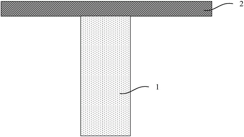
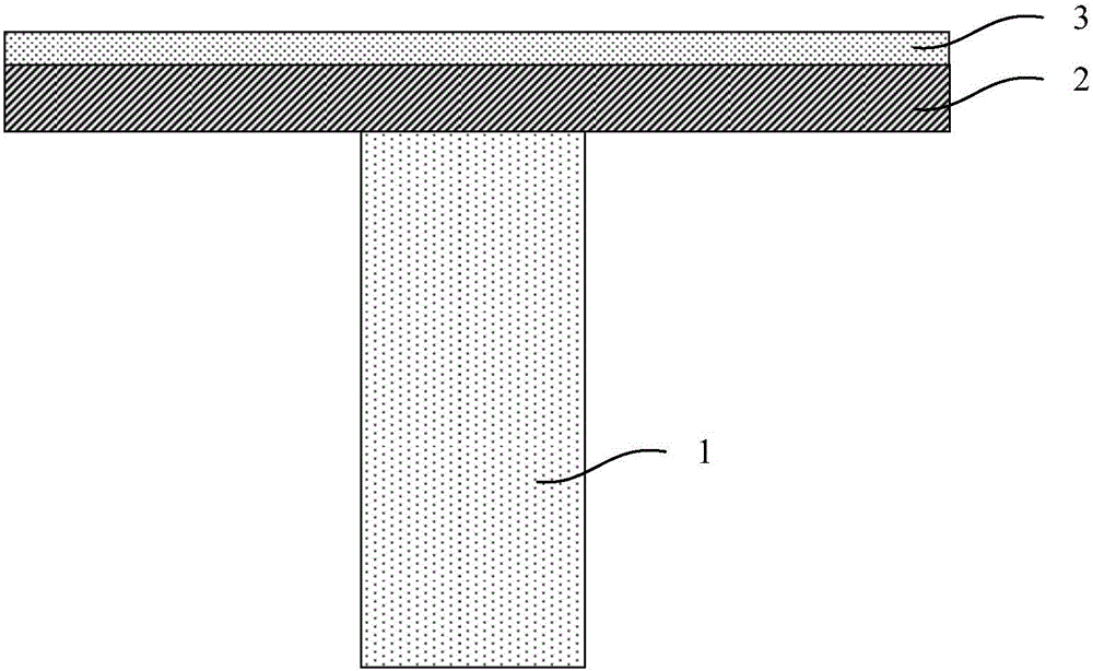
[0044] see Figure 1 ~ Figure 4 , the present invention also provides a preparation method of a phase-change memory cell, the phase-change memory adopts the Cr-doped Ge 2 Sb 2 Te 5 A phase change material, the method comprising the steps of:

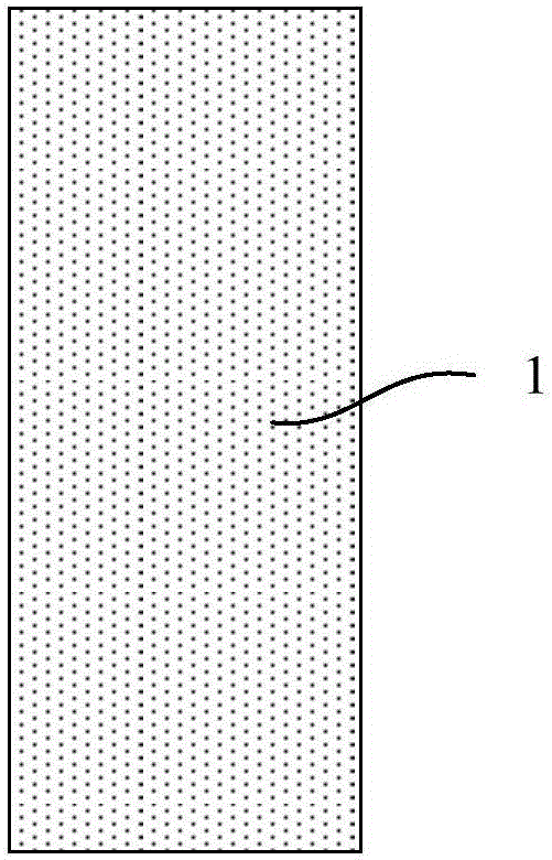
[0045] See first figure 1 , performing step S1: forming the lower electrode layer 1 .

[0046] Specifically, sputtering, evaporation, chemical vapor deposition, plasma enhanced chemical vapor deposition, low pressure chemical vapor deposition, metal compound vapor deposition, molecular beam epitaxy, atomic vapor deposition or atomic layer deposition can be used The lower electrode layer 1 is prepared by any method, and the lower electrode layer 1 is preferably prepared by the CVD method in this embodiment. The material of the lower electrode layer 1 can be one of the single metal materials W, Pt, Au, Ti, Al, Ag, Cu or Ni, or an alloy composed of any two or more of the single metal materials material, or the nitride or oxide of the ...

Embodiment 3

[0058]In this embodiment, the phase change memory unit prepared in the second embodiment is tested. see Figure 5 , which is shown as the voltage change curve (V-I diagram) of a certain device unit under the action of current excitation. It can be seen that as the current increases, the voltage value rises steadily at first, and when the current value reaches about 5 μA, the voltage value suddenly drops, indicating that the material undergoes a phase transition at this time, rapidly changing from an amorphous state to a crystalline state. Afterwards, as the current increased, the voltage value increased slightly and then stabilized, indicating that the crystallization process was further fully carried out. It can be seen that based on the new phase change material Cr 1 Ge 2 Sb 2 Te 5 The device unit has a threshold current / voltage of about 5μA / 1.2V.

[0059] See Figure 6 , is the relationship between the measured device unit resistance and the applied pulse voltage, us...


PUM

PropertyMeasurementUnit
Thicknessaaaaaaaaaa
Diameteraaaaaaaaaa
Heightaaaaaaaaaa

Abstract

The invention provides a Cr-doped Ge2Sb2Te5 phase change material, a phase change memory unit and a preparation method. The ingredient general formula of the Cr-doped Ge2Sb2Te5 phase change material is CrxGe2Sb2Te5, wherein x is an atomic ratio of the Cr element, and x is more than 0.5 and less than 1.5. Cr doping in Ge2Sb2Te5 is carried out, Cr is a kind of metal with an extremely high melting point, heat stability of a phase change material can be raised, Cr can form bonds with Ge, Sb and Te, so segregation is avoided effectively. Under action of external energy, the Cr-doped Ge2Sb2Te5 phase change material can achieve reversible conversion between high resistance state and low resistance state, and the resistance value ratio of the high resistance state to the low resistance state can reach about two orders of magnitudes. When the phase change material is employed as a memory media of a phase change memory, the phase change memory unit has advantages of fast phase change speed, low write operation current and the like, and high temperature data retentivity and reliability of the device are raised greatly. The phase change memory employing the phase change memory unit structure has advantages of high speed, low power consumption, good data retentivity and the like.

Description

technical field [0001] The invention belongs to the technical field of micro-nano electronics and relates to a Cr-doped Ge 2 Sb 2 Te 5 Phase change material, phase change memory unit and preparation method thereof. Background technique [0002] In the semiconductor market, memory occupies an important position. Phase change memory using phase change thin film material as storage medium is considered to be the most potential next-generation non-volatile memory. Phase-change memory technology is based on the Ovshinsky electronic effect memory proposed by S.R.Ovshinsky in the late 1960s and early 1970s. Its key materials include phase-change films as storage media, heating electrode materials, insulating materials and lead-out electrodes. materials etc. The basic principle of phase change memory is: apply electrical pulse signal to the device unit, make the phase change material produce reversible transition between the amorphous state and the crystalline state, use the ma...

Claims


Application Information

Patent Timeline
IPC IPC(8): H01L45/00C23C14/35
CPCC23C14/35H10N70/231H10N70/011
Inventor 王青刘波夏洋洋张中华宋三年宋志棠封松林
Owner SHANGHAI INST OF MICROSYSTEM & INFORMATION TECH CHINESE ACAD OF SCI
Why Eureka
Try Eureka