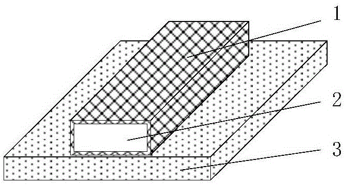
On-chip inductor based on graphene/metal composite wire and preparation method
A metal composite, on-chip inductor technology, used in semiconductor/solid-state device manufacturing, circuits, electrical components, etc., can solve difficult problems, achieve the effect of improving quality factor, strong practicability, and simple process
- Summary
- Abstract
- Description
- Claims
- Application Information
AI Technical Summary
Problems solved by technology
Method used
Image
Examples
Embodiment 1
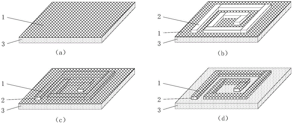
[0044] 1) Prepare a piece of PET film, wash and dry it; use chemical vapor deposition to grow a nine-layer graphene film doped with nitrogen impurities on the nickel foil; use the graphene transfer process to transfer the nine-layer graphene film on the nickel foil to PET film, such as figure 2 as shown in (a);
[0045]Electron beam evaporation is used to deposit a layer of 2um aluminum film on the PET film with graphene transferred, and the aluminum film is etched into an aluminum inductor coil by photolithography and wet etching processes, such as figure 2 as shown in (b);
[0046] 2) A nine-layer graphene film doped with nitrogen impurities is grown on a nickel foil by chemical vapor deposition; a graphene transfer process is used to transfer the nine-layer graphene on the nickel foil to a PET film prepared with an aluminum inductor coil, such as figure 2 as shown in (c);
[0047] 3) The graphene film transferred to the PET film is etched by photolithography process a...
Embodiment 2
[0049] 1) Prepare a quartz plate, clean it, and dry it; use chemical vapor deposition to grow three-layer graphene doped with boron impurities on nickel foil; use graphene transfer process to transfer the three-layer graphene on copper foil to the quartz plate ,Such as figure 2 as shown in (a);
[0050] A layer of 2um aluminum film is deposited on the quartz sheet with graphene transferred by electron beam evaporation process, and the aluminum film is etched into aluminum inductance coil by photolithography process and wet etching process, such as figure 2 as shown in (b);
[0051] 2) Three-layer graphene doped with boron impurities is grown on nickel foil by chemical vapor deposition; three-layer graphene on nickel foil is transferred to a quartz sheet prepared with an aluminum inductance coil by a graphene transfer process, such as figure 2 as shown in (c);
[0052] 3) The graphene film transferred to the quartz sheet is etched by photolithography process and oxygen pl...
Embodiment 3
[0054] 1) Prepare a piece of quartz, clean and dry;
[0055] A layer of 2um copper film is deposited on the quartz wafer by magnetron sputtering; the copper film is patterned by photolithography and wet etching to form a copper inductance coil, such as image 3 as shown in (a);
[0056] 2) Put the quartz plate with the copper inductance coil into the chemical vapor deposition system, introduce hydrogen gas at a flow rate of 15 sccm, raise the temperature to 1024°C within 60 minutes, and keep it for 15 minutes; then fill it with methane gas at a flow rate of 30 sccm, and keep the temperature constant After 15 minutes, slowly cool down to 700°C at a rate of 1°C / min, turn off the methane gas, and the graphene growth stage is completed. At this point, the single-layer graphene grows on the surface of the copper wire to form a Figure 4 The structure of the semi-wrapped composite wire is shown; the temperature is rapidly cooled to room temperature, and the flow of hydrogen gas is ...
PUM
| Property | Measurement | Unit |
|---|---|---|
| Conductivity | aaaaa | aaaaa |
| Line width | aaaaa | aaaaa |
Abstract
Description
Claims
Application Information
 - R&D
- Intellectual Property
- Life Sciences
- Materials
- Tech Scout
- Unparalleled Data Quality
- Higher Quality Content
- 60% Fewer Hallucinations
Browse by: Latest US Patents, China's latest patents, Technical Efficacy Thesaurus, Application Domain, Technology Topic, Popular Technical Reports.
© 2025 PatSnap. All rights reserved.Legal|Privacy policy|Modern Slavery Act Transparency Statement|Sitemap|About US| Contact US: help@patsnap.com


